Check out my first novel, midnight's simulacra!
Sandy Bridge: Difference between revisions
| (6 intermediate revisions by the same user not shown) | |||
| Line 1: | Line 1: | ||
[[File:Sandybridge.jpg|thumb|right|Sandy Bridge microarchitecture]] | [[File:Sandybridge.jpg|thumb|right|Sandy Bridge microarchitecture]] | ||
[[File:Sandybridgedie.jpg|thumb|right|Sandy Bridge die]] | [[File:Sandybridgedie.jpg|thumb|right|Sandy Bridge die]] | ||
Intel released Sandy Bridge in January 2011 as a major revision of [[Nehalem]]. Core i7 and i5 models were released simultaneously; a 2011-02 drop will include i3's. All released and planned Sandy Bridge packages support on-die integrated [http://en.wikipedia.org/wiki/Intel_GMA GMA-HD2] graphics processors and make use of the new [http://en.wikipedia.org/wiki/LGA_1155 LGA 1155] ("H2") socket, a successor to [http://en.wikipedia.org/wiki/LGA_1156 LGA 1156] ("Socket H"). The P67, H67, Q67 and B65 chipsets ("Platform Controller Hub" or PCH in recent Intel terminology) have been released to support Sandy Bridge, and are compatible with all current variants. It uses the scalable ring-based bus designed for [[Larrabee]] (introduced on [[Nehalem|Nehalem EX]]) and supports [[AVX]] and [[AES-NI]] instructions. Sandy Bridge processors (and their on-die IGPs) use a 32nm process ([[Ivy Bridge]], a planned minor successor to Sandy Bridge, will use 22nm process). | Intel released Sandy Bridge in January 2011 as a major revision of [[Nehalem]]. Core i7 and i5 models were released simultaneously; a 2011-02 drop will include i3's. All released and planned Sandy Bridge packages support on-die integrated [http://en.wikipedia.org/wiki/Intel_GMA GMA-HD2] graphics processors and make use of the new [http://en.wikipedia.org/wiki/LGA_1155 LGA 1155] ("H2") socket, a successor to [http://en.wikipedia.org/wiki/LGA_1156 LGA 1156] ("Socket H"). The "Cougar Point" line -- P67, H67, Z68, Q67 and B65 chipsets ("Platform Controller Hub" or PCH in recent Intel terminology) have been released to support Sandy Bridge, and are compatible with all current variants. It uses the scalable ring-based bus designed for [[Larrabee]] (introduced on [[Nehalem|Nehalem EX]]) and supports [[AVX]] and [[AES-NI]] instructions. Sandy Bridge processors (and their on-die IGPs) use a 32nm process ([[Ivy Bridge]], a planned minor successor to Sandy Bridge, will use 22nm process). | ||
==Architecture== | ==Architecture== | ||
| Line 86: | Line 86: | ||
===IGP=== | ===IGP=== | ||
GMA HD2 improves transcendental math hardware over HD1, and expands the register file. The 2000-series IGP has 6 execution units, while the 3000 has 12. Currently, 3000-series IGP's are reserved for K-series processors (the P67 performance-oriented chipset cannot make use of the IGP, and requires a discrete graphics adapter). The IGP has limited locking on its clock -- the H67 chipset can control IGP multipliers. | GMA HD2 improves transcendental math hardware over HD1, and expands the register file. The 2000-series IGP has 6 execution units, while the 3000 has 12. Currently, 3000-series IGP's are reserved for K-series processors (the P67 performance-oriented chipset cannot make use of the IGP, and requires a discrete graphics adapter). The IGP has limited locking on its clock -- the H67 chipset can control IGP multipliers. | ||
Unlike [[Larrabee]]'s fully programmable shaders (suitable for [[GPGPU]]), Sandy Bridge IGP | Unlike [[Larrabee]]'s fully programmable shaders (suitable for [[GPGPU]]), Sandy Bridge IGP devotes significant space to fixed-function components. The instruction set is said to closely parallel the DirectX 10 API. There are a fixed 120 registers per thread, as opposed to the dynamically partitionable register file of previous Intel HD Graphics. Intel HD is a valid [[OpenCL]] target. | ||
The IGP runs on its own voltage and frequency planes, and supports its own [[Turbo Boost]]. It supports [[HDMI]] 1.4. | The IGP runs on its own voltage and frequency planes, and supports its own [[Turbo Boost]]. It supports [[HDMI]] 1.4. | ||
<blockquote>Two key versions of graphics will be available, Intel® HD Graphics 2000 and Intel® HD Graphics 3000/3000+, with Intel® HD Graphics 2000 targeting lower voltage (lower power) applications and Intel® HD Graphics 3000 a more mainstream set of applications. -- [http://software.intel.com/en-us/articles/intel-graphics-developers-guides/ Intel Graphics Developer Guide]</blockquote> | <blockquote>Two key versions of graphics will be available, Intel® HD Graphics 2000 and Intel® HD Graphics 3000/3000+, with Intel® HD Graphics 2000 targeting lower voltage (lower power) applications and Intel® HD Graphics 3000 a more mainstream set of applications. -- [http://software.intel.com/en-us/articles/intel-graphics-developers-guides/ Intel Graphics Developer Guide]</blockquote> | ||
====Intel HD Graphics==== | |||
[[File:intelhdarch.png|right|thumb|Intel HD architecture]] | |||
At the heart of Intel HD is an array of "Execution Units", unified SMT SIMD shaders with unified transcendental units. Fixed-function hardware covers clipping and setup/early-z, as well as decoding of vertex, pixel and geometry shaders (these last are fed by the "Command Streamer", which also feeds video processing, the 2d unit, and display hardware). | |||
===MFX=== | ====MFX==== | ||
The Multi-Format Codec (MFX) engine is fixed functionality for high-performance, low-power transcoding. It features intensely parallel hardware. | The Multi-Format Codec (MFX) engine is fixed functionality for high-performance, low-power transcoding. It features intensely parallel hardware. | ||
| Line 106: | Line 108: | ||
** The Intel H67 Express Chipset Platform Block Diagram does claim that GMA-HD will not be available on all processors | ** The Intel H67 Express Chipset Platform Block Diagram does claim that GMA-HD will not be available on all processors | ||
** ...but none are currently planned for release. | ** ...but none are currently planned for release. | ||
* The Z68 chipset, scheduled for release in Q2 2011, addresses these issues | |||
==Sources== | ==Sources== | ||
* "[http://www.realworldtech.com/page.cfm?ArticleID=RWT080811195102 Intel's Sandy Bridge Graphics Architecture]", Real World Technologies, 2011-08-08 | |||
* "[http://techreport.com/articles.x/20190 Introducing the P67 Express]", The Tech Report, 2011-01-04 (Geoff Gasior) | * "[http://techreport.com/articles.x/20190 Introducing the P67 Express]", The Tech Report, 2011-01-04 (Geoff Gasior) | ||
* "[http://www.pcper.com/article.php?aid=1057 Intel Core i7-2600K (and friends) Sandy Bridge Processor Review]", PC Perspective, 2011-01-02 (Ryan Shrout) | * "[http://www.pcper.com/article.php?aid=1057 Intel Core i7-2600K (and friends) Sandy Bridge Processor Review]", PC Perspective, 2011-01-02 (Ryan Shrout) | ||
Latest revision as of 19:03, 17 February 2012
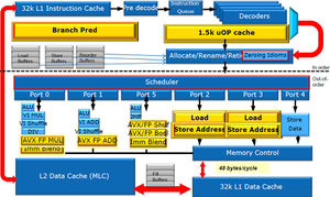
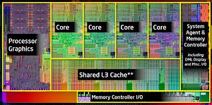
Intel released Sandy Bridge in January 2011 as a major revision of Nehalem. Core i7 and i5 models were released simultaneously; a 2011-02 drop will include i3's. All released and planned Sandy Bridge packages support on-die integrated GMA-HD2 graphics processors and make use of the new LGA 1155 ("H2") socket, a successor to LGA 1156 ("Socket H"). The "Cougar Point" line -- P67, H67, Z68, Q67 and B65 chipsets ("Platform Controller Hub" or PCH in recent Intel terminology) have been released to support Sandy Bridge, and are compatible with all current variants. It uses the scalable ring-based bus designed for Larrabee (introduced on Nehalem EX) and supports AVX and AES-NI instructions. Sandy Bridge processors (and their on-die IGPs) use a 32nm process (Ivy Bridge, a planned minor successor to Sandy Bridge, will use 22nm process).
Architecture
Sandy Bridge is the first Intel processor to support AVX instructions, including the 256-bit YMM0..15 registers and the VEX instruction encoding.
- XSAVE/XRSTOR operations will properly preserve and restore the full 256-bit registers.
- May be called from any processor state. Use the XSAVE/XRSTOR memory areas, specified by MSRs.
- XMM SSE registers map to the lower 128 bit of the corresponding YMM registers; the upper 128 bits will be zeroed out by SSE instructions.
Microarchitecture
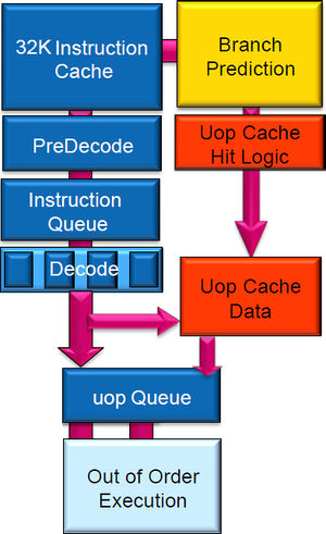
See my architecture page for background information.
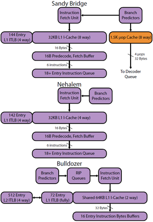
- As opposed to Nehalem's Loop Stream Decoder, there's a simple (ie always-used) 8-way/32-set/LRU 1536-μop cache (6 μops per line)
- Unlike the P4's trace cache, we're caching at instruction granularity, not trace (superblock)
- Also, we're lazily flushed, as opposed to on every context/VM switch
- Augments 8-way/32K VIPT L1 icache (completely distinct hardware)
- L1TLB: 16 full-assoc dedicated per-thread large pages, 128 4-way core-shared small pages
- (FIXME: in HT-incapable processor models, do you get 16 or 32 large pages per core?)
- Branch prediction can use multiple target sizes, depending on relative distance, and multiple history widths, depending on branch variance
- 2 dataload/addrstore ports are now dataload/addrload/addrstore
- 100MHz Turbo Boost increments as compared to Nehalem's 133Mhz, and more bins when multiple cores are in use
Instruction Window
- New physical register file (PRF) outside the OOO core (RRF) contains all in-flight operands; ops in window carry pointers only
- Likely motivator: 256-bit operand width of AVX instructions
- There's a PRF for FP and integer vectors, and one for pure 64-bit integers
- A return to the much-maligned NetBurst architecture! (Core architecture replaced PRF's with RRF's)
- Downside: need for dereferencing hardware (done via deeper pipelines, not longer cycles -- higher stall/flush costs)
- Load buffers: 48 -> 64
- Store buffers: 32 -> 36
- Reservation stations: 30 -> 54
- ROB entries: 128 -> 168
Last-Level Cache

- Shared LLC remains "sliced" (NUMA), with slices distributed among cores
- Off-slice accesses can contend
- L3 LLC moved out of "uncore" and now runs at core frequency
- Downclocked cores mean the L3 can be underclocked relative to the IGP!
- Cache access queue ("cache controller") is per-slice, rather than global to the cache
- L3 latencies reduced
- Less latency for lookup due to shorter tags under slicing
- L3 lies in core clock/voltage domain rather than uncore
- Frequency is (usually) higher in core domains
- Penalty for signals crossing frequency/voltage domains eliminated
- Latency for off-slice access increases as more hops are added
- Three coherency domains
- CPU: coherent
- Graphics: incoherent area is managed by driver, made coherent via synchronization
- Non-coherent: incoherent
"GPU write caches need to be flushed before writing to buffers with the CPU. GPU read caches only need to be invalidated when changed in a non-coherent cache domain. GPU write caches may need to be flushed for the results to reach scanout. Solution: track which cache domain the buffer has dirty cache lines in, and which read cache domains the buffer has had invalidated since the last write." -- Eric Anholt, "Linux Graphics Driver Development"
Interconnect
- Larrabee's ring interconnect connects the cores, IGP, LLC slices, media engine and System Agent (northbridge). Four 32-byte rings (plus ECC bits) are used:
- Data, Request, ACK, Snoop
- Interconnect is built directly into L3 cache
- Fully pipelined at core clock frequency
- Adding more cores thus adds more bandwidth
- ...but also increases latency, and exacerbates certain contention patterns
Branding/Differentiation
See Intel's product matrix for complete, up-to-date information. Sandy Bridge retains Core i{7,5,3} families, but uses a four-digit model number beginning with 2, followed by an optional suffix.
- Core i7 exhibits the highest clock speeds and largest speedups from Turbo Boost. It uses SMT and provides vPro and AES-NI instructions.
- Core i5 does not support SMT. The Core i5-2500K does not support vPro, while other Core i5's do.
- Core i3 does not support Turbo Boost, vPro, or AES-NI. It *does* support SMT.
Core i7 and Core i5 Sandy Bridge processors are thus far either quad- or dual-core, while Core i3 is strictly dual-core. Assuming SMT to be enabled where possible, this means Core i7 provides 8 execution units, while Core i5 and Core i3 both provide 4. Without HyperThreading, the Core i3 provides 2, while the others provide 4. Currently, the Core i3 is limited to 3MB of cache, while Core i5/i7 support up to 8MB (current i5's ship with no more than 6MB).
Release Sets
- 2011-01-09 saw the first set of Sandy Bridge processors.
- TDP range: 45--96W. Freq range: 2.1GHz--3.4GHz, 3GHz--3.8GHz. Quad cores with 6--8MB LLC.
- i7-2720QM, i5-2300, i5-2400, i5-2400S, i5-2500, i5-2500K, i5-2500S, i5-2500T, i7-2600, i7-2600K, i7-2600S, i7-2820QM, i7-2920XM, i7-2710QE, i7-2715QE
- 2011-02-20 sees a second set, with more mobile options (and the first Sandy Bridge Core i3's).
- TDP range: 17W--65W. Freq range: 1.4GHz--3.3GHz, 3--3.3GHz. Dual cores with 3--6MB LLC.
- i5-2540M, i5-2520M, i7-2620M, i3-2100, i3-2100T, i3-2120, i5-2390T, i5-2510E, i7-2629M, i7-2649M, i7-2657M, i7-2617M, i5-2537M, i5-2515E
K: unlocked S: performance-optimized T: power-optimized M: mobile Q: quad X: eXtreme E: embedded
Processor Support
Northbridge ("System Agent")
- Different clock and power plane
- Provides an IOMMU
- 16 PCIe 2.0 lanes (2x16b @ 5GT/s)
- Dual-channel DDR3 (2x8b @ FSB x KT/s)
IGP
GMA HD2 improves transcendental math hardware over HD1, and expands the register file. The 2000-series IGP has 6 execution units, while the 3000 has 12. Currently, 3000-series IGP's are reserved for K-series processors (the P67 performance-oriented chipset cannot make use of the IGP, and requires a discrete graphics adapter). The IGP has limited locking on its clock -- the H67 chipset can control IGP multipliers.
Unlike Larrabee's fully programmable shaders (suitable for GPGPU), Sandy Bridge IGP devotes significant space to fixed-function components. The instruction set is said to closely parallel the DirectX 10 API. There are a fixed 120 registers per thread, as opposed to the dynamically partitionable register file of previous Intel HD Graphics. Intel HD is a valid OpenCL target.
The IGP runs on its own voltage and frequency planes, and supports its own Turbo Boost. It supports HDMI 1.4.
Two key versions of graphics will be available, Intel® HD Graphics 2000 and Intel® HD Graphics 3000/3000+, with Intel® HD Graphics 2000 targeting lower voltage (lower power) applications and Intel® HD Graphics 3000 a more mainstream set of applications. -- Intel Graphics Developer Guide
Intel HD Graphics
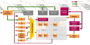
At the heart of Intel HD is an array of "Execution Units", unified SMT SIMD shaders with unified transcendental units. Fixed-function hardware covers clipping and setup/early-z, as well as decoding of vertex, pixel and geometry shaders (these last are fed by the "Command Streamer", which also feeds video processing, the 2d unit, and display hardware).
MFX
The Multi-Format Codec (MFX) engine is fixed functionality for high-performance, low-power transcoding. It features intensely parallel hardware.
Chipset
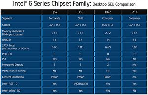
Chipsets are currently using a 65nm process. The PCH is connected to the processor via a 20Gb/s (2x4b@2.5GT/s) Direct Media Interface 2.0 bus. The P67 explicitly supports unlocked (overclockable) memory, power and cores (only K-series i7 and i5 processors provide unlocked multipliers, thus a P67+K-series is required for core overclocking). The P67 does not support the IGP, but does provide lane-splitting for SLI/CrossFire setups. While the H67 locks the FSB to 1333MHz, the P67 can likely use DDR3-1600, DDR3-1866 and DDR3-2133. The 6-series chipsets integrate a clock (rather than using a discrete motherboard source) and signal it over DMI (hence the new socket).
Implications
It's impossible to fully utilize the hardware capabilities of K-series processors or P67 motherboards.
- The K-series touts two advantages: an unlocked clock multiplier, and a 3000-series IGP. To take advantage of the unlocked multiplier, a P67 PCH is required, but the P67 does not support the IGP (overclockers are presumed, I suppose, to use discrete GPUs)!
- The P67 supports only LGA 1155 processors thus far, all of which have IGPs unusable by the P67.
- The Intel H67 Express Chipset Platform Block Diagram does claim that GMA-HD will not be available on all processors
- ...but none are currently planned for release.
- The Z68 chipset, scheduled for release in Q2 2011, addresses these issues
Sources
- "Intel's Sandy Bridge Graphics Architecture", Real World Technologies, 2011-08-08
- "Introducing the P67 Express", The Tech Report, 2011-01-04 (Geoff Gasior)
- "Intel Core i7-2600K (and friends) Sandy Bridge Processor Review", PC Perspective, 2011-01-02 (Ryan Shrout)
- "Intel's Sandy Bridge Architecture Exposed", AnandTech, 2010-09-14 (Anand Lal Shimpi)
- "Sandy Bridge: Intel's Next-Generation Architecture Revealed", ExtremeTech, 2010-09-20 (Matthew Murray)
- "Sandy Bridge Products" at http://www.intel.com
- "Intel's Sandy Bridge Microarchitecture" at Real World Technologies, 2010-09-25 (David Kanter)
- "Intel Graphics Developer Guide", 321671-005US, 2011-01