Check out my first novel, midnight's simulacra!
Haswell
From dankwiki

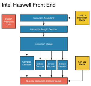
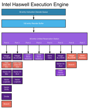
Haswell follows Ivy Bridge, the die-shrunk "Tock" of Intel's Nehalem. It will be manufactured on a 22nm process, and is scheduled to be released in Q1 2013. Haswell will feature transactional memory, and represents a major step forward in power reduction, largely through new ACPI sleep states ("S0ix states") and improvements throughout the associated chipset ("Shark Bay").

See Also
- "Intel's Haswell Architecture Analyzed: Building a New PC and a New Intel", Anandtech, 2012-10-05
- "Analysis of Transactional Memory in Haswell", Real World Technologies, 2012-02-15
- "Transactional Synchronization in Haswell", Intel SDN, 2012-02-07