Check out my first novel, midnight's simulacra!
Sandy Bridge: Difference between revisions
No edit summary |
No edit summary |
||
| Line 1: | Line 1: | ||
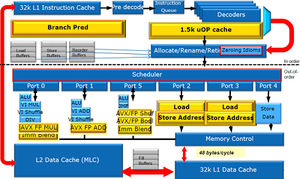
[[File:Sandybridge.jpg|thumb|right|Sandy Bridge microarchitecture]] | [[File:Sandybridge.jpg|thumb|right|Sandy Bridge microarchitecture]] | ||
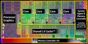
[[File:Sandybridgedie.jpg|thumb|right|Sandy Bridge die]] | |||
Intel released Sandy Bridge in January 2011 as the major successor to [[Nehalem]]. Core i7, i5 and i3 variants were released simultaneously. Sandy Bridge can support an on-die integrated graphics processor. All Sandy Bridge processors to date use the new LGA 1155 socket ("Socket H2"), the successor to LGA 1156 ("Socket H"). The P67, H67, and H61 chipsets have been released to support Sandy Bridge, and are compatible with all current variants. It exhibits the ring-based bus designed for [[Larrabee]] (introduced on [[Nehalem|Nehalem EX]]) and supports [[AVX]] instructions. Sandy Bridge processors (and their on-die IGP) are based on a 32nm process. | Intel released Sandy Bridge in January 2011 as the major successor to [[Nehalem]]. Core i7, i5 and i3 variants were released simultaneously. Sandy Bridge can support an on-die integrated graphics processor. All Sandy Bridge processors to date use the new LGA 1155 socket ("Socket H2"), the successor to LGA 1156 ("Socket H"). The P67, H67, and H61 chipsets have been released to support Sandy Bridge, and are compatible with all current variants. It exhibits the ring-based bus designed for [[Larrabee]] (introduced on [[Nehalem|Nehalem EX]]) and supports [[AVX]] instructions. Sandy Bridge processors (and their on-die IGP) are based on a 32nm process. | ||
Revision as of 04:19, 12 January 2011


Intel released Sandy Bridge in January 2011 as the major successor to Nehalem. Core i7, i5 and i3 variants were released simultaneously. Sandy Bridge can support an on-die integrated graphics processor. All Sandy Bridge processors to date use the new LGA 1155 socket ("Socket H2"), the successor to LGA 1156 ("Socket H"). The P67, H67, and H61 chipsets have been released to support Sandy Bridge, and are compatible with all current variants. It exhibits the ring-based bus designed for Larrabee (introduced on Nehalem EX) and supports AVX instructions. Sandy Bridge processors (and their on-die IGP) are based on a 32nm process.
Microarchitecture
- As opposed to Nehalem's Loop Stream Decoder, there's a simple, direct-mapped/LRU 1.5k μop cache
- Branch prediction can use multiple target sizes, depending on relative distance, and multiple history widths, depending on branch variance
Last-Level Cache
- Shared LLC remains "sliced" (NUMA), with slices distributed among cores
- L3 LLC moved out of uncore and now runs at core frequency
- Downclocked cores mean the L3 can be underclocked relative to the IGP!
- Cache pipeline is per-slice, rather than global to the cache
- L3 latencies reduced
Interconnect
- Larrabee's ring interconnect connects the cores, IGP, LLC slices, media engine and System Agent (northbridge). 4 32-byte rings are used:
- Data, Request, ACK, Snoop
- Interconnect is built directly into L3 cache
Family
- Core i7 exhibits the highest clock speeds and largest speedups from Turbo Boost. It uses SMT and provides vPro and AES-NI instructions.
- Core i5 does not support SMT. The Core i5-2500K does not support vPro, while other Core i5's do.
- Core i3 does not support Turbo Boost, vPro, or AES-NI. It *does* support SMT.
All current Core i7 and Core i5 Sandy Bridge processors are quad-core, while Core i3 is dual-core. Assuming SMT to be enabled where possible, this means Core i7 provides 8 execution units, while Core i5 and Core i3 both provide 4. Without HyperThreading, the Core i3 provides 2, while the others provide 4. Currently, the Core i3 is limited to 3MB of cache, while Core i5/i7 support up to 8MB (current i5's ship with 6MB).
Processor Support
Northbridge ("System Agent")
- Different clock and power plane
- Provides an IOMMU
- 16 PCIe 2.0 lanes
- Dual-channel DDR3
IGP
The 2000-series IGP has 6 execution units, while the 3000 has 12. Currently, 3000-series IGP's are reserved for K-series processors (the P67 performance-oriented chipset cannot make use of the IGP, and requires a discrete graphics adapter). The IGP has limited locking on its clock -- the H67 chipset can control IGP multipliers.
Unlike Larrabee's fully programmable shaders (suitable for GPGPU), Sandy Bridge IGP makes extensive use of fixed-function components. The instruction set is said to closely parallel the DirectX 10 API. There are a fixed 120 registers per thread, as opposed to the dynamically partitionable register file of previous Intel HD Graphics.
MFX
The Multi-Format Codec (MFX) engine is fixed functionality for high-performance, low-power transcoding. It features intensely parallel hardware.
Chipset
Chipsets are currently using a 65nm process. The chipset is connected to the processor via a 20Gb/s Direct Media Interconnect. The P67 chipset provides 16 more PCIe lanes than H67, and explicitly supports unlocked (overclockable) memory, power and cores (only K-series i7 and i5 processors provide unlocked multipliers, thus a P67+K-series is required for core overclocking). It does not support the IGP, but does provide lane-splitting for SLI/CrossFire setups.
Sources
- "Introducing the P67 Express", The Tech Report, 2011-01-04
- "Intel Core i7-2600K (and friends) Sandy Bridge Processor Review", PC Perspective, 2011-01-02
- "Intel's Sandy Bridge Architecture Exposed", AnandTech, 2010-09-14
- "Sandy Bridge: Intel's Next-Generation Architecture Revealed", ExtremeTech, 2010-09-20