| [ Team LiB ] |


|
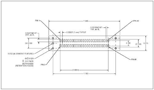
Slot Connector vs. Mid-Bus PadThe PCI Express bus can also be used for chip-to-chip connections. In this case, there are no connectors for the analyzer to plug into. This requires a mid-bus probing technique. The mid-bus probing does not allow for bus exercising since the bus stubs can create signal integrity issues. Developers wanting to characterize their products by fully exercising it should design a development card that includes their device and plug it into the Exerciser for characterization and verification. Figure A-15 on page 978 illustrates one recommended interface to help developers and tool vendors to provide a common interface for analysis. However, this interface design is not part of the specifications and is intended only for prototype boards and does not include all required details at this time. Figure A-15. Mid-bus Pad DefinitionThe exact implementation on how to mount the probe to the pads needs to be resolved or recommended by the development tool vendors. In this diagram only the position and sizes of mounting holes are defined
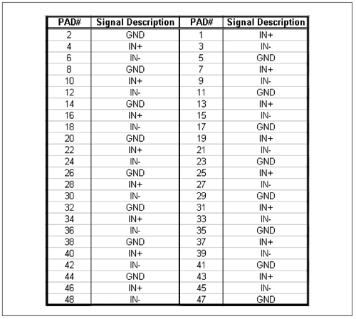
This interface is referred to as mid-bus probing and it defines a mechanical specification for the set of pads to probe the signals, mostly for chip-to-chip buses. The figure indicates the mechanical pads that must be designed on the board if they are interested in using a mid-bus probe to analyze the bus. Suggested signal assignments for the probe are not defined in the specifications. Figure A-16 is a proposed suggestion that tool vendors are considering. Since there is an effect on the signals, the probe vendor must provide specifications of the probe loading effects and the developers must also consider these effects. Figure A-16. Mid-Bus Suggested Signal Assignment
System developers must confirm with their analyzer/probe vendor to be sure that the probe vendor is also using the same signal assignment.  |
| [ Team LiB ] |
|