Signal Integrity, Design and Measurement
General
The PCI Express bus runs at 2.5Gb/s and it should be noted that, without a proper PCB design, developers will not be able to produce a functional product. At these frequencies the losses impact the quality of the signal that passes through the transmission medium. Additional sources of problems may also be attributed to crosstalk. In short, more extensive research on high-speed design guidelines and simulation by system modeling are strongly recommended. Here are a few items that first time designers of Gigahertz technology should be aware of and pursue.
High Speed PCB Design Requirements
The designer must be aware of:
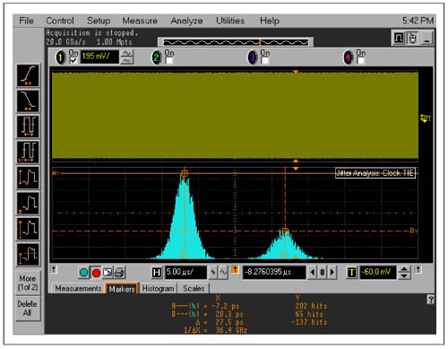
Symmetrical routing and trace length matching There are requirements for routing such as that high speed signals must be routed as a symmetrical pair with a difference of less than 20 mil between the two traces. These traces also need to be impedance controlled to 100 Ohm differential, or 50 Ohm single ended. Bend control The high speed signals should also avoid sharp bends such as 90 degrees. The PCI Express signal integrity is based on controlling loss through the interconnect media as much as other factors. Via Stitching Stitching is recommended to keep the number of vias for high speed signals to a minimum (such as two for add-in cards). It is sometimes a practice to add a ground via next to the signal via to keep a uniform continuation for the return path (referred to as via stitching). Jitter control One of the most common issues in signal integrity is controlling the jitter. A frequent source of jitter in a serial data stream is the reference clock. Jitter generally occurs due to excessive noise on the VCC supply for clock distribution circuits and PCI Express transceivers. Proper filtering and decoupling for the power supply and around the clock oscillators and buffers must be implemented to keep the DC noise to a few millivolts in order to keep the jitter, and therefore the Eye pattern, of the output signals to an acceptable level. Also, clock sources (on board oscillators) must be of a high stability and low jitter. Figure A-20 on page 986 is a screenshot of a measurement made on a clock to show the acceptable jitter, and Figure A-21 on page 987 represents unacceptable jitter.
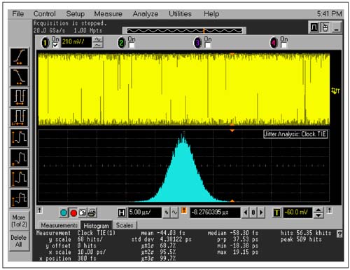
This measurement indicates a clock jitter of 39ps P-P and a stable clock at the desired frequency.
This measurement indicates a high clock jitter along with an unstable frequency.
The absolute jitter and stability is highly dependent on device specification requirements. Developers need to know the acceptable limits of their devices and use the measurement results accordingly.
 |

