Check out my first novel, midnight's simulacra!
Haswell: Difference between revisions
Jump to navigation
Jump to search
add real world tech link |
No edit summary |
||
| (7 intermediate revisions by the same user not shown) | |||
| Line 1: | Line 1: | ||
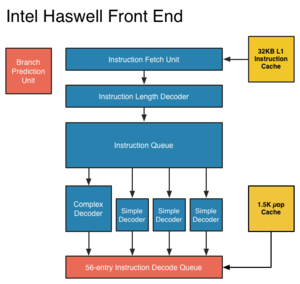
Haswell follows [[Ivy Bridge]], the die-shrunk "[[Tick-Tock|Tock]]" of Intel's [[Nehalem]]. It will be manufactured on a 22nm process, and is scheduled to be released in Q1 2013. Haswell will feature [[transactional memory]]. | [[File:Haswellfrontend.png|right|thumb|Haswell frontend. Note the unified decode queue compared to the SMT-split queue of [[Ivy Bridge]]. ]] | ||
Haswell follows [[Ivy Bridge]], the die-shrunk "[[Tick-Tock|Tock]]" of Intel's [[Nehalem]]. It will be manufactured on a 22nm process, and is scheduled to be released in Q1 2013. Haswell will feature [[transactional memory]], and represents a major step forward in power reduction, largely through new [[ACPI]] sleep states ("S0ix states") and improvements throughout the associated chipset ("Shark Bay"). Haswell supports [[AVX|AVX2]] instructions (including the FMA set) on two ports, doubling both single and double-precision AVX floating point flops over [[Ivy Bridge]]. | |||
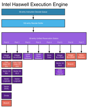
[[File:Haswellexec.png|right|thumb|Haswell employs an 8-wide ALU.]] | |||
==See Also== | ==See Also== | ||
* "[http://www.anandtech.com/show/6355/intels-haswell-architecture Intel's Haswell Architecture Analyzed: Building a New PC and a New Intel]", Anandtech, 2012-10-05 | |||
* "[http://www.realworldtech.com/page.cfm?ArticleID=RWT021512050738 Analysis of Transactional Memory in Haswell]", Real World Technologies, 2012-02-15 | * "[http://www.realworldtech.com/page.cfm?ArticleID=RWT021512050738 Analysis of Transactional Memory in Haswell]", Real World Technologies, 2012-02-15 | ||
* "[http://software.intel.com/en-us/blogs/2012/02/07/transactional-synchronization-in-haswell/ Transactional Synchronization in Haswell]", Intel SDN, 2012-02-07 | * "[http://software.intel.com/en-us/blogs/2012/02/07/transactional-synchronization-in-haswell/ Transactional Synchronization in Haswell]", Intel SDN, 2012-02-07 | ||
[[CATEGORY: X86]] | [[CATEGORY: X86]] | ||
Latest revision as of 13:22, 1 December 2012

Haswell follows Ivy Bridge, the die-shrunk "Tock" of Intel's Nehalem. It will be manufactured on a 22nm process, and is scheduled to be released in Q1 2013. Haswell will feature transactional memory, and represents a major step forward in power reduction, largely through new ACPI sleep states ("S0ix states") and improvements throughout the associated chipset ("Shark Bay"). Haswell supports AVX2 instructions (including the FMA set) on two ports, doubling both single and double-precision AVX floating point flops over Ivy Bridge.

See Also
- "Intel's Haswell Architecture Analyzed: Building a New PC and a New Intel", Anandtech, 2012-10-05
- "Analysis of Transactional Memory in Haswell", Real World Technologies, 2012-02-15
- "Transactional Synchronization in Haswell", Intel SDN, 2012-02-07