Check out my first novel, midnight's simulacra!
Haswell: Difference between revisions
Jump to navigation
Jump to search
No edit summary |
No edit summary |
||
| Line 2: | Line 2: | ||
Haswell follows [[Ivy Bridge]], the die-shrunk "[[Tick-Tock|Tock]]" of Intel's [[Nehalem]]. It will be manufactured on a 22nm process, and is scheduled to be released in Q1 2013. Haswell will feature [[transactional memory]], and represents a major step forward in power reduction, largely through new [[ACPI]] sleep states ("S0ix states") and improvements throughout the associated chipset ("Shark Bay"). | Haswell follows [[Ivy Bridge]], the die-shrunk "[[Tick-Tock|Tock]]" of Intel's [[Nehalem]]. It will be manufactured on a 22nm process, and is scheduled to be released in Q1 2013. Haswell will feature [[transactional memory]], and represents a major step forward in power reduction, largely through new [[ACPI]] sleep states ("S0ix states") and improvements throughout the associated chipset ("Shark Bay"). | ||
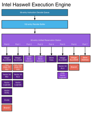
[[File:Haswellexec.png|right|thumb|Haswell employs an 8-wide ALU.]] | |||
==See Also== | ==See Also== | ||
* "[http://www.anandtech.com/show/6355/intels-haswell-architecture Intel's Haswell Architecture Analyzed: Building a New PC and a New Intel]", Anandtech, 2012-10-05 | * "[http://www.anandtech.com/show/6355/intels-haswell-architecture Intel's Haswell Architecture Analyzed: Building a New PC and a New Intel]", Anandtech, 2012-10-05 | ||
Revision as of 13:14, 1 December 2012

Haswell follows Ivy Bridge, the die-shrunk "Tock" of Intel's Nehalem. It will be manufactured on a 22nm process, and is scheduled to be released in Q1 2013. Haswell will feature transactional memory, and represents a major step forward in power reduction, largely through new ACPI sleep states ("S0ix states") and improvements throughout the associated chipset ("Shark Bay").

See Also
- "Intel's Haswell Architecture Analyzed: Building a New PC and a New Intel", Anandtech, 2012-10-05
- "Analysis of Transactional Memory in Haswell", Real World Technologies, 2012-02-15
- "Transactional Synchronization in Haswell", Intel SDN, 2012-02-07