| [ Team LiB ] |


|
Predecessor Buses ComparedIn an effort to compare and contrast features of predecessor buses, the next section of this chapter describes some of the key features of IO bus architectures defined by the PCI Special Interest Group (PCISIG). These buses, shown in Table 1-1 on page 12, include the PCI 33 MHz bus, PCI- 66 MHz bus, PCI-X 66 MHz/133 MHz buses, PCI-X 266/533 MHz buses and finally PCI Express.
Author's DisclaimerIn comparing these buses, it is not the authors' intention to suggest that any one bus is better than any other bus. Each bus architecture has its advantages and disadvantages. After evaluating the features of each bus architecture, a particular bus architecture may turn out to be more suitable for a specific application than another bus architecture. For example, it is the system designers responsibility to determine whether to implement a PCI-X bus or PCI Express for the I/O interconnect in a high-end server design. Our goal in this chapter is to document the features of each bus architecture so that the designer can evaluate the various bus architectures. Bus Performances and Number of Slots ComparedTable 1-2 on page 13 shows the various bus architectures defined by the PCISIG. The table shows the evolution of bus frequencies and bandwidths. As is obvious, increasing bus frequency results in increased bandwidth. However, increasing bus frequency compromises the number of electrical loads or number of connectors allowable on a bus at that frequency. At some point, for a given bus architecture, there is an upper limit beyond which one cannot further increase the bus frequency, hence requiring the definition of a new bus architecture.
PCI Express Aggregate ThroughputA PCI Express interconnect that connects two devices together is referred to as a Link. A Link consists of either x1, x2, x4, x8, x12, x16 or x32 signal pairs in each direction. These signals are referred to as Lanes. A designer determines how many Lanes to implement based on the targeted performance benchmark required on a given Link. Table 1-3 shows aggregate bandwidth numbers for various Link width implementations. As is apparent from this table, the peak bandwidth achievable with PCI Express is significantly higher than any existing bus today. Let us consider how these bandwidth numbers are calculated. The transmission/reception rate is 2.5 Gbits/sec per Lane per direction. To support a greater degree of robustness during data transmission and reception, each byte of data transmitted is converted into a 10-bit code (via an 8b/10b encoder in the transmitter device). In other words, for every Byte of data to be transmitted, 10-bits of encoded data are actually transmitted. The result is 25% additional overhead to transmit a byte of data. Table 1-3 accounts for this 25% loss in transmission performance. PCI Express implements a dual-simplex Link which implies that data is transmitted and received simultaneously on a transmit and receive Lane. The aggregate bandwidth assumes simultaneous traffic in both directions. To obtain the aggregate bandwith numbers in Table 1-3 multiply 2.5 Gbits/sec by 2 (for each direction), then multiply by number of Lanes, and finally divide by 10-bits per Byte (to account for the 8-to-10 bit encoding).
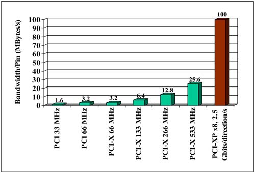
Performance Per Pin ComparedAs is apparent from Figure 1-1, PCI Express achieves the highest bandwidth per pin. This results in a device package with fewer pins and a motherboard implementation with few wires and hence overall reduced system cost per unit bandwidth. Figure 1-1. Comparison of Performance Per Pin for Various Buses
In Figure 1-1, the first 7 bars are associated with PCI and PCI-X buses where we assume 84 pins per device. This includes 46 signal pins, interrupt and power management pins, error pins and the remainder are power and ground pins. The last bar associated with a x8 PCI Express Link assumes 40 pins per device which include 32 signal lines (8 differential pairs per direction) and the rest are power and ground pins. |
| [ Team LiB ] |
|