| [ Team LiB ] |


|
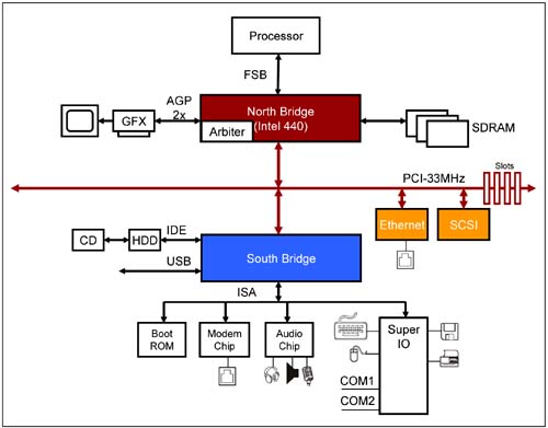
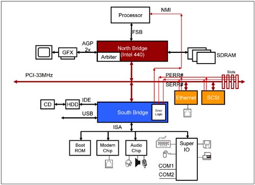
I/O Bus Architecture Perspective33 MHz PCI Bus Based SystemFigure 1-2 on page 17 is a 33 MHz PCI bus based system. The PCI system consists of a Host (CPU) bus-to-PCI bus bridge, also referred to as the North bridge. Associated with the North bridge is the system memory bus, graphics (AGP) bus, and a 33 MHz PCI bus. I/O devices share the PCI bus and are connected to it in a multi-drop fashion. These devices are either connected directly to the PCI bus on the motherboard or by way of a peripheral card plugged into a connector on the bus. Devices connected directly to the motherboard consume one electrical load while connectors are accounted for as 2 loads. A South bridge bridges the PCI bus to the ISA bus where slower, lower performance peripherals exist. Associated with the south bridge is a USB and IDE bus. A CD or hard disk is associated with the IDE bus. The South bridge contains an interrupt controller (not shown) to which interrupt signals from PCI devices are connected. The interrupt controller is connected to the CPU via an INTR signal or an APIC bus. The South bridge is the central resource that provides the source of reset, reference clock, and error reporting signals. Boot ROM exists on the ISA bus along with a Super IO chip, which includes keyboard, mouse, floppy disk controller and serial/parallel bus controllers. The PCI bus arbiter logic is included in the North bridge. Figure 1-2. 33 MHz PCI Bus Based Platform
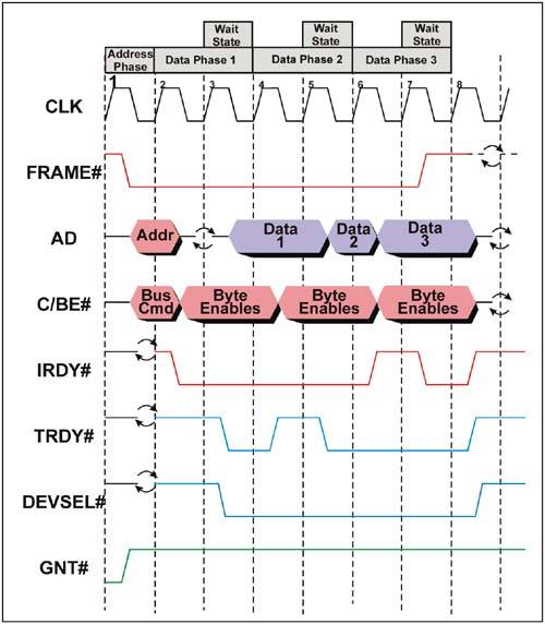
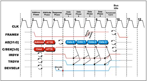
Figure 1-3 on page 18 represents a typical PCI bus cycle. The PCI bus clock is 33 MHz. The address bus width is 32-bits (4GB memory address space), although PCI optionally supports 64-bit address bus. The data bus width is implemented as either 32-bits or 64-bits depending on bus performance requirement. The address and data bus signals are multiplexed on the same pins (AD bus) to reduce pin count. Command signals (C/BE#) encode the transaction type of the bus cycle that master devices initiate. PCI supports 12 transaction types that include memory, IO, and configuration read/write bus cycles. Control signals such as FRAME#, DEVSEL#, TRDY#, IRDY#, STOP# are handshake signals used during bus cycles. Finally, the PCI bus consists of a few optional error related signals, interrupt signals and power management signals. A PCI master device implements a minimum of 49 signals. Figure 1-3. Typical PCI Burst Memory Read Bus Cycle
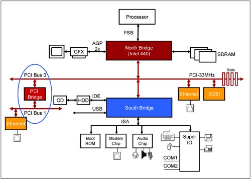
Any PCI master device that wishes to initiate a bus cycle first arbitrates for use of the PCI bus by asserting a request (REQ#) to the arbiter in the North bridge. After receiving a grant (GNT#) from the arbiter and checking that the bus is idle, the master device can start a bus cycle. Electrical Load Limit of a 33 MHz PCI BusThe PCI specification theoretically supports 32 devices per PCI bus. This means that PCI enumeration software will detect and recognize up to 32 devices per bus. However, as a rule of thumb, a PCI bus can support a maximum of 10-12 electrical loads (devices) at 33 MHz. PCI implements a static clocking protocol with a clock period of 30 ns at 33 MHz. PCI implements reflected-wave switching signal drivers. The driver drives a half signal swing signal on the rising edge of PCI clock. The signal propagates down the PCI bus transmission line and is reflected at the end of the transmission line where there is no termination. The reflection causes the half swing signal to double. The doubled (full signal swing) signal must settle to a steady state value with sufficient setup time prior to the next rising edge of PCI clock where receiving devices sample the signal. The total time from when a driver drives a signal until the receiver detects a valid signal (including propagation time and reflection delay plus setup time) must be less than the clock period of 30 ns. The more electrical loads on a bus, the longer it takes for the signal to propagate and double with sufficient setup to the next rising edge of clock. As mentioned earlier, a 33 MHz PCI bus meets signal timing with no more than 10-12 loads. Connectors on the PCI bus are counted as 2 loads because the connector is accounted for as one load and the peripheral card with a PCI device is the second load. As indicated in Table 1-2 on page 13 a 33 MHz PCI bus can be designed with a maximum of 4-5 connectors. To connect any more than 10-12 loads in a system requires the implementation of a PCI-to-PCI bridge as shown in Figure 1-4. This permits an additional 10-12 loads to be connected on the secondary PCI bus 1. The PCI specification theoretically supports up to 256 buses in a system. This means that PCI enumeration software will detect and recognize up to 256 PCI bridges per system. Figure 1-4. 33 MHz PCI Based System Showing Implementation of a PCI-to-PCI Bridge
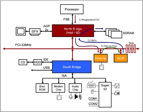
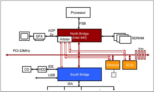
PCI Transaction Model - Programmed IOConsider an example in which the CPU communicates with a PCI peripheral such as an Ethernet device shown in Figure 1-5. Transaction 1 shown in the figure, which is initiated by the CPU and targets a peripheral device, is referred to as a programmed IO transaction. Software commands the CPU to initiate a memory or IO read/write bus cycle on the host bus targeting an address mapped in a PCI device's address space. The North bridge arbitrates for use of the PCI bus and when it wins ownership of the bus generates a PCI memory or IO read/write bus cycle represented in Figure 1-3 on page 18. During the first clock of this bus cycle (known as the address phase), all target devices decode the address. One target (the Ethernet device in this example) decodes the address and claims the transaction. The master (North bridge in this case) communicates with the claiming target (Ethernet controller). Data is transferred between master and target in subsequent clocks after the address phase of the bus cycle. Either 4 bytes or 8 bytes of data are transferred per clock tick depending on the PCI bus width. The bus cycle is referred to as a burst bus cycle if data is transferred back-to-back between master and target during multiple data phases of that bus cycle. Burst bus cycles result in the most efficient use of PCI bus bandwidth. Figure 1-5. PCI Transaction Model
At 33 MHz and the bus width of 32-bits (4 Bytes), peak bandwidth achievable is 4 Bytes x 33 MHz = 133 MBytes/sec. Peak bandwidth on a 64-bit bus is 266 Mbytes/sec. See Table 1-2 on page 13. Efficiency of the PCI bus for data payload transport is in the order of 50%. Efficiency is defined as number of clocks during which data is transferred divided by the number of total clocks, times 100. The lost performance is due to bus idle time between bus cycles, arbitration time, time lost in the address phase of a bus cycle, wait states during data phases, delays during transaction retries (not discussed yet), as well as latencies through PCI bridges. PCI Transaction Model - Direct Memory Access (DMA)Data transfer between a PCI device and system memory is accomplished in two ways: The first less efficient method uses programmed IO transfers as discussed in the previous section. The PCI device generates an interrupt to inform the CPU that it needs data transferred. The device interrupt service routine (ISR) causes the CPU to read from the PCI device into one of its own registers. The ISR then tells the CPU to write from its register to memory. Similarly, if data is to be moved from memory to the PCI device, the ISR tells the CPU to read from memory into its own register. The ISR then tells the CPU to write from its register to the PCI device. It is apparent that the process is very inefficient for two reasons. First, there are two bus cycles generated by the CPU for every data transfer, one to memory and one to the PCI device. Second, the CPU is busy transferring data rather than performing its primary function of executing application code. The second more efficient method to transfer data is the DMA (direct memory access) method illustrated by Transaction 2 in Figure 1-5 on page 20, where the PCI device becomes a bus master. Upon command by a local application (software) which runs on a PCI peripheral or the PCI peripheral hardware itself, the PCI device may initiate a bus cycle to talk to memory. The PCI bus master device (SCSI device in this example) arbitrates for the PCI bus, wins ownership of the bus and initiates a PCI memory bus cycle. The North bridge which decodes the address acts as the target for the transaction. In the data phase of the bus cycle, data is transferred between the SCSI master and the North bridge target. The bridge in turn generates a DRAM bus cycle to communicate with system memory. The PCI peripheral generates an interrupt to inform the system software that the data transfer has completed. This bus master or DMA method of data transport is more efficient because the CPU is not involved in the data move and further only one burst bus cycle is generated to move a block of data. PCI Transaction Model - Peer-to-PeerA Peer-to-peer transaction shown as Transaction 3 in Figure 1-5 on page 20 is the direct transfer of data between two PCI devices. A master that wishes to initiate a transaction, arbitrates, wins ownership of the bus and starts a transaction. A target PCI device that recognizes the address claims the bus cycle. For a write bus cycle, data is moved from master to target. For a read bus cycle, data is moved from target to master. PCI Bus ArbitrationA PCI device that wishes to initiate a bus cycle arbitrates for use of the bus first. The arbiter implements an arbitration algorithm with which it decides who to grant the bus to next. The arbiter is able to grant the bus to the next requesting device while a bus cycle is in progress. This arbitration protocol is referred to as hidden bus arbitration. Hidden bus arbitration allows for more efficient hand over of the bus from one bus master device to another with only one idle clock between two bus cycles (referred to as back-to-back bus cycles). PCI protocol does not provide a standard mechanism by which system software or device drivers can configure the arbitration algorithm in order to provide for differentiated class of service for various applications. Figure 1-6. PCI Bus Arbitration
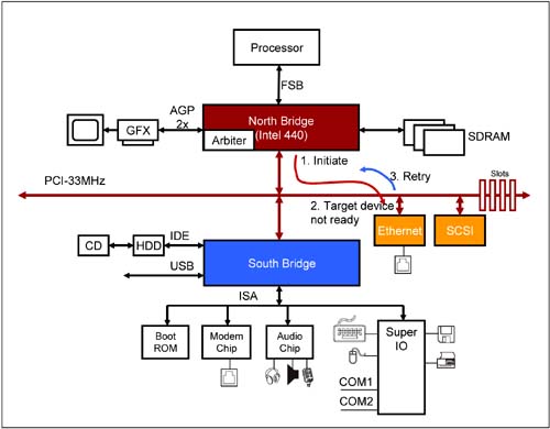
PCI Delayed Transaction ProtocolPCI Retry ProtocolWhen a PCI master initiates a transaction to access a target device and the target device is not ready, the target signals a transaction retry. This scenario is illustrated in Figure 1-7. Figure 1-7. PCI Transaction Retry Mechanism
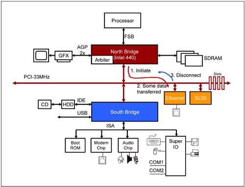
Consider the following example in which the North bridge initiates a memory read transaction to read data from the Ethernet device. The Ethernet target claims the bus cycle. However, the Ethernet target does not immediately have the data to return to the North bridge master. The Ethernet device has two choices by which to delay the data transfer. The first is to insert wait-states in the data phase. If only a few wait-states are needed, then the data is still transferred efficiently. If however the target device requires more time (more than 16 clocks from the beginning of the transaction), then the second option the target has is to signal a retry with a signal called STOP#. A retry tells the master to end the bus cycle prematurely without transferring data. Doing so prevents the bus from being held for a long time in wait-states, which compromises the bus efficiency. The bus master that is retried by the target waits a minimum of 2 clocks and must once again arbitrate for use of the bus to re-initiate the identical bus cycle. During the time that the bus master is retried, the arbiter can grant the bus to other requesting masters so that the PCI bus is more efficiently utilized. By the time the retried master is granted the bus and it re-initiates the bus cycle, hopefully the target will claim the cycle and will be ready to transfer data. The bus cycle goes to completion with data transfer. Otherwise, if the target is still not ready, it retries the master's bus cycle again and the process is repeated until the master successfully transfers data. PCI Disconnect ProtocolWhen a PCI master initiates a transaction to access a target device and if the target device is able to transfer at least one doubleword of data but cannot complete the entire data transfer, it disconnects the bus cycle at the point at which it cannot continue the data transfer. This scenario is illustrated in Figure 1-8. Figure 1-8. PCI Transaction Disconnect Mechanism
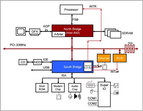
Consider the following example in which the North bridge initiates a burst memory read transaction to read data from the Ethernet device. The Ethernet target device claims the bus cycle and transfers some data, but then runs out of data to transfer. The Ethernet device has two choices to delay the data transfer. The first option is to insert wait-states during the current data phase while waiting for additional data to arrive. If the target needs to insert only a few wait-states, then the data is still transferred efficiently. If however the target device requires more time (the PCI specification allows maximum of 8 clocks in the data phase), then the target device must signal a disconnect. To do this the target asserts STOP# in the middle of the bus cycle to tell the master to end the bus cycle prematurely. A disconnect results in some data is transferred, while a retry does not. Disconnect frees the bus from long periods of wait states. The disconnected master waits a minimum of 2 clocks before once again arbitrating for use of the bus and continuing the bus cycle at the disconnected address. During the time that the bus master is disconnected, the arbiter may grant the bus to other requesting masters so that the PCI bus is utilized more efficiently. By the time the disconnected master is granted the bus and continues the bus cycle, hopefully the target is ready to continue the data transfer until it is completed. Otherwise, the target once again retries or disconnects the master's bus cycle and the process is repeated until the master successfully transfers all its data. PCI Interrupt HandlingCentral to the PCI interrupt handling protocol is the interrupt controller shown in Figure 1-9. PCI devices use one-of-four interrupt signals (INTA#, INTB#, INTC#, INTD#) to trigger an interrupt request to the interrupt controller. In turn, the interrupt controller asserts INTR to the CPU. If the architecture supports an APIC (Advanced Programmable Interrupt Controller) then it sends an APIC message to the CPU as opposed to asserting the INTR signal. The interrupted CPU determines the source of the interrupt, saves its state and services the device that generated the interrupt. Interrupts on PCI INTx# signals are sharable. This allows multiple devices to generate their interrupts on the same interrupt signal. OS software has the overhead to determine which one of the devices sharing the interrupt signal generated the interrupt. This is accomplished by polling the Interrupt Pending bit mapped in a device's memory space. Doing so incurs additional latency in servicing the interrupting device. Figure 1-9. PCI Interrupt Handling
PCI Error HandlingPCI devices are optionally designed to detect address and data phase parity errors during transactions. Even parity is generated on the PAR signal during each bus cycle's address and data phases. The device that receives the address or data during a bus cycle uses the parity signal to determine if a parity error has occurred due to noise on the PCI bus. If a device detects an address phase parity error, it asserts SERR#. If a device detects a data phase parity error, it asserts PERR#. The PERR# and SERR# signals are connected to the error logic (in the South bridge) as shown in Figure 1-10 on page 27. In many systems, the error logic asserts the NMI signal (non-maskable interrupt signal) to the CPU upon detecting PERR# or SERR#. This interrupt results in notification of a parity error and the system shuts down (We all know the blue screen of death). Kind of draconian don't you agree? Figure 1-10. PCI Error Handling Protocol
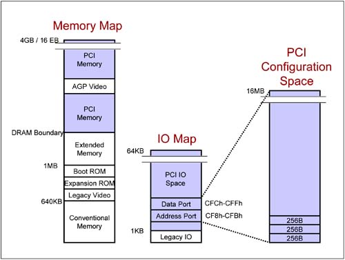
Unfortunately, PCI error detection and reporting is not robust. PCI errors are fatal uncorrectable errors that many times result in system shutdown. Further, errors are detectable as long as an odd number of signals are affected by noise. Given the poor PCI error detection protocol and error handling policies, many system designs either disable or do not support error checking and reporting. PCI Address Space MapPCI architecture supports 3 address spaces shown in Figure 1-11. These are the memory, IO and configuration address spaces. The memory address space goes up to 4 GB for systems that support 32-bit memory addressing and optionally up to 16 EB (exabytes) for systems that support 64-bit memory addressing. PCI supports up to 4GB of IO address space, however, many platforms limit IO space to 64 KB due to X86 CPUs only supporting 64 KB of IO address space. PCI devices are configured to map to a configurable region within either the memory or IO address space. Figure 1-11. Address Space Mapping
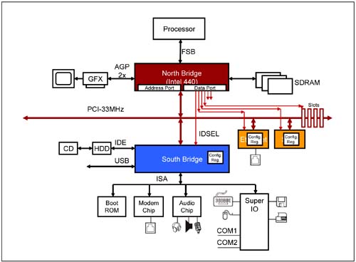
PCI device configuration registers map to a third space called configuration address space. Each PCI function may have up to 256 Bytes of configuration address space. The configuration address space is 16 MBytes. This is calculated by multiplying 256 Bytes, by 8 functions per device, by 32 devices per bus, by 256 buses per system. An x86 CPU can access memory or IO address space but does not support configuration address space directly. Instead, CPUs access PCI configuration space indirectly by indexing through an IO mapped Address Port and Data Port in the host bridge (North bridge or MCH). The Address Port is located at IO address CF8h-CFBh and the Data Port is mapped to location CFCh-CFFh. PCI Configuration Cycle GenerationPCI configuration cycle generation involves two steps.
The address for the configuration transaction address phase is obtained from the contents of the Address register. During the configuration bus cycle, one of the point-to-point IDSEL signals shown in Figure 1-12 on page 29 is asserted to select the device whose register is being accessed. That PCI target device claims the configuration cycle and fulfills the request. Figure 1-12. PCI Configuration Cycle Generation
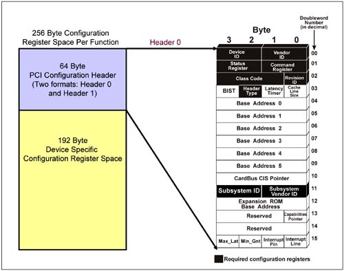
PCI Function Configuration Register SpaceEach PCI device contains up to 256 Bytes of configuration register space. The first 64 bytes are configuration header registers and the remainding 192 Bytes are device specific registers. The header registers are configured at boot time by the Boot ROM configuration firmware and by the OS. The device specific registers are configured by the device's device driver that is loaded and executed by the OS at boot time. Figure 1-13. 256 Byte PCI Function Configuration Register Space
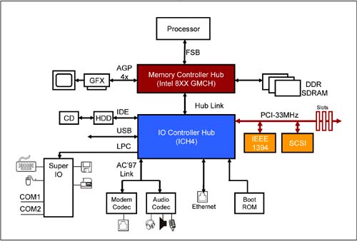
Within the header space, the Base Address registers are one of the most important registers configured by the 'Plug and Play' configuration software. It is via these registers that software assigns a device its memory and/or IO address space within the system's memory and IO address space. No two devices are assigned the same address range, thus ensuring the 'plug and play' nature of the PCI system. PCI Programming ModelSoftware instructions may cause the CPU to generate memory or IO read/write bus cycles. The North bridge decodes the address of the resulting CPU bus cycles, and if the address maps to PCI address space, the bridge in turn generates a PCI memory or IO read/write bus cycle. A target device on the PCI bus claims the cycle and completes the transfer. In summary, the CPU communicates with any PCI device via the North bridge, which generates PCI memory or IO bus cycles on the behalf of the CPU. An intelligent PCI device that includes a local processor or bus master state machine (typically intelligent IO cards) can also initiate PCI memory or IO transactions on the PCI bus. These masters can communicate directly with any other devices, including system memory associated with the North bridge. A device driver executing on the CPU configures the device-specific configuration register space of an associated PCI device. A configured PCI device that is bus master capable can initiate its own transactions, which allows it to communicate with any other PCI target device including system memory associated with the North bridge. The CPU can access configuration space as described in the previous section. PCI Express architecture assumes the identical programming model as the PCI programming model described above. In fact, current OSs written for PCI systems can boot a PCI Express system. Current PCI device drivers will initialize PCI Express devices without any driver changes. PCI configuration and enumeration firmware will function unmodified on a PCI Express system. Limitations of a 33 MHz PCI SystemAs indicated in Table 1-2 on page 13, peak bandwidth achievable on a 64-bit 33 MHz PCI bus is 266 Mbytes/sec. Current high-end workstation and server applications require greater bandwidth. Applications such as gigabit Ethernet and high performance disc transfers in RAID and SCSI configurations require greater bandwidth capability than the 33 MHz PCI bus offers. Latest Generation of Intel PCI ChipsetsFigure 1-14 shows an example of a later generation Intel PCI chipset. The two shaded devices are NOT the North bridge and South bridge shown in earlier diagrams. Instead, one device is the Memory Controller Hub (MCH) and the other is the IO Controller Hub (ICH). The two chips are connected by a proprietary Intel high throughput, low pin count bus called the Hub Link. Figure 1-14. Latest Generation of PCI Chipsets
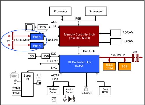
The ICH includes the South bridge functionality but does not support the ISA bus. Other buses associated with ICH include LPC (low pin count) bus, AC'97, Ethernet, Boot ROM, IDE, USB, SMbus and finally the PCI bus. The advantage of this architecture over previous architectures is that the IDE, USB, Ethernet and audio devices do not transfer their data through the PCI bus to memory as is the case with earlier chipsets. Instead they do so through the Hub Link. Hub Link is a higher performance bus compared to PCI. In other words, these devices bypass the PCI bus when communicating with memory. The result is improved performance. 66 MHz PCI Bus Based SystemHigh end systems that require better IO bandwidth implement a 66 MHz 64-bit PCI buses. This PCI bus supports peak data transfer rate of 533 MBytes/sec. The PCI 2.1 specification released in 1995 added 66MHz PCI support. Figure 1-15 shows an example of a 66 MHz PCI bus based system. This system has similar features to that described in Figure 1-14 on page 32. However, the MCH chip in this example supports two additional Hub Link buses that connect to P64H (PCI 64-bit Hub) bridge chips, providing access to the 64-bit, 66 MHz buses. These buses each support 1 connector in which a high-end peripheral card may be installed. Figure 1-15. 66 MHz PCI Bus Based Platform
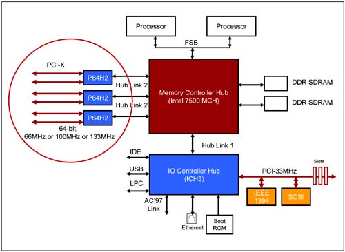
Limitations of 66 MHz PCI busThe PCI clock period at 66 MHz is 15 ns. Recall that PCI supports reflected-wave signaling drivers that are weaker drivers, which have slower rise and fall times as compared to incident-wave signaling drivers. It is a challenge to design a 66 MHz device or system that satisfies the signal timing requirements. A 66 MHz PCI based motherboard is routed with shorter signal traces to ensure shorter signal propagation delays. In addition, the bus is loaded with fewer loads in order to ensure faster signal rise and fall times. Taking into account typical board impedances and minimum signal trace lengths, it is possible to interconnect a maximum of four to five 66 MHz PCI devices. Only one or two connectors may be connected on a 66 MHz PCI bus. This is a significant limitation for a system which requires multiple devices interconnected. The solution requires the addition of PCI bridges and hence multiple buses to interconnect devices. This solution is expensive and consumes additional board real estate. In addition, transactions between devices on opposite sides of a bridge complete with greater latency because bridges implement delayed transactions. This requires bridges to retry all transactions that must cross to the other side (with the exception of memory writes which are posted). Limitations of PCI ArchitectureThe maximum frequency achievable with the PCI architecture is 66 MHz. This is a result of the static clock method of driving and latching signals and because reflected-wave signaling is used. PCI bus efficiency is in the order of 50% or 60%. Some of the factors that contribute towards this reduced efficiency are listed below. The PCI specification allows master and target devices to insert wait-states during data phases of a bus cycle. Slow devices will add wait-states which reduces the efficiency of bus cycles. PCI bus cycles do not indicate transfer size. This makes buffer management within master and target devices inefficient. Delayed transactions on PCI are handled inefficiently. When a master is retried, it guesses when to try again. If the master tries too soon, the target may retry the transaction again. If the master waits too long to retry, the latency to complete a data transfer is increased. Similarly, if a target disconnects a transaction the master must guess when to resume the bus cycle at a later time. All PCI bus master accesses to system memory result in a snoop access to the CPU cache. Doing so results in additional wait states during PCI bus master accesses of system memory. The North bridge or MCH must assume all system memory address space is cachable even though this may not be the case. PCI bus cycles provide no mechanism by which to indicate an access to non-cachable memory address space. PCI architecture observes strict ordering rules as defined by the specification. Even if a PCI application does not require observation of these strict ordering rules, PCI bus cycles do not provide a mechanism to allow relaxed ordering rule. Observing relaxed ordering rules allows bus cycles (especially those that cross a bridge) to complete with reduced latency. PCI interrupt handling architecture is inefficient especially because multiple devices share a PCI interrupt signal. Additional software latency is incurred while software discovers which device or devices that share an interrupt signal actually generated the interrupt. The processor's NMI interrupt input is asserted when a PCI parity or system error is detected. Ultimately the system shuts down when an error is detected. This is a severe response. A more appropriate response might be to detect the error and attempt error recovery. PCI does not require error recovery features, nor does it support an extensive register set for documenting a variety of detectable errors. These limitations above have been resolved in the next generation bus architectures, namely PCI-X and PCI Express. 66 MHz and 133 MHz PCI-X 1.0 Bus Based PlatformsFigure 1-16 on page 36 is an example of an Intel 7500 server chipset based system. This chipset has similarities to the 8XX chipset described earlier. MCH and ICH chips are connected via a Hub Link 1.0 bus. Associated with ICH is a 32-bit 33 MHz PCI bus. The 7500 MCH chip includes 3 additional high performance Hub Link 2.0 ports. These Hub Link ports are connected to 3 Hub Link-to-PCI-X Hub 2 bridges (P64H2). Each P64H2 bridge supports 2 PCI-X buses that can run at frequencies up to 133MHz. Hub Link 2.0 Links can sustain the higher bandwidth requirements for PCI-X traffic that targets system memory. Figure 1-16. 66 MHz/133 MHz PCI-X Bus Based Platform
PCI-X FeaturesThe PCI-X bus is a higher frequency, higher performance, higher efficiency bus compared to the PCI bus. PCI-X devices can be plugged into PCI slots and vice-versa. PCI-X and PCI slots employ the same connector format. Thus, PCI-X is 100% backwards compatible to PCI from both a hardware and software standpoint. The device drivers, OS, and applications that run on a PCI system also run on a PCI-X system. PCI-X signals are registered. A registered signal requires smaller setup time to sample the signal as compared with a non-registered signal employed in PCI. Also, PCI-X devices employ PLLs that are used to pre-drive signals with smaller clock-to-out time. The time gained from reduced setup time and clock-to-out time is used towards increased clock frequency capability and the ability to support more devices on the bus at a given frequency compared to PCI. PCI-X supports 8-10 loads or 4 connectors at 66 MHz and 3-4 loads or 1-2 connectors at 133 MHz. The peak bandwidth achievable with 64-bit 133 MHz PCI-X is 1064 MBytes/sec. Following the first data phase, the PCI-X bus does not allow wait states during subsequent data phases. Most PCI-X bus cycles are burst cycles and data is generally transferred in blocks of no less than 128 Bytes. This results in higher bus utilization. Further, the transfer size is specified in the attribute phase of PCI-X transactions. This allows for more efficient device buffer management. Figure 1-17 is an example of a PCI-X burst memory read transaction. Figure 1-17. Example PCI-X Burst Memory Read Bus Cycle
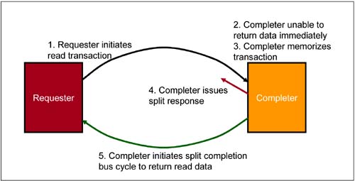
PCI-X Requester/Completer Split Transaction ModelConsider an example of the split transaction protocol supported by PCI-X for delaying transactions. This protocol is illustrated in Figure 1-18. A requester initiates a read transaction. The completer that claims the bus cycles may be unable to return the requested data immediately. Rather than signaling a retry as would be the case in PCI protocol, the completer memorizes the transaction (address, transaction type, byte count, requester ID are memorized) and signals a split response. This prompts the requester to end the bus cycle, and the bus goes idle. The PCI-X bus is now available for other transactions, resulting in more efficient bus utilization. Meanwhile, the requester simply waits for the completer to supply it the requested data at a later time. Once the completer has gathered the requested data, it then arbitrates and obtains bus ownership and initiates a split completion bus cycle during which it returns the requested data. The requester claims the split completion bus cycle and accepts the data from the completer. Figure 1-18. PCI-X Split Transaction Protocol
The split completion bus cycle is very much like a write bus cycle. Exactly two bus transactions are needed to complete the entire data transfer. In between these two bus transactions (the read request and the split completion transaction) the bus is utilized for other transactions. The requester also receives the requested data in a very efficient manner. PCI Express architecture employs a similar transaction protocol. These performance enhancement features described so far contribute towards an increased transfer efficiency of 85% for PCI-X as compared to 50%-60% with PCI protocol. PCI-X devices must support Message Signaled Interrupt (MSI) architecture, which is a more efficient architecture than the legacy interrupt architecture described in the PCI architecture section. To generate an interrupt request, a PCI-X devices initiates a memory write transaction targeting the Host (North) bridge. The data written is a unique interrupt vector associated with the device generating the interrupt. The Host bridge interrupts the CPU and the vector is delivered to the CPU in a platform specific manner. With this vector, the CPU is immediately able to run an interrupt service routine to service the interrupting device. There is no software overhead in determining which device generated the interrupt. Also, unlike in the PCI architecture, no interrupt pins are required. PCI Express architecture implements the MSI protocol, resulting in reduced interrupt servicing latency and elimination of interrupt signals. PCI Express architecture also supports the RO bit and NS bit feature with the result that those transactions with either NS=1 or RO=1 complete with better performance than transactions with NS=0 or RO=0. PCI transactions by definition assume NS=0 and RO=0.
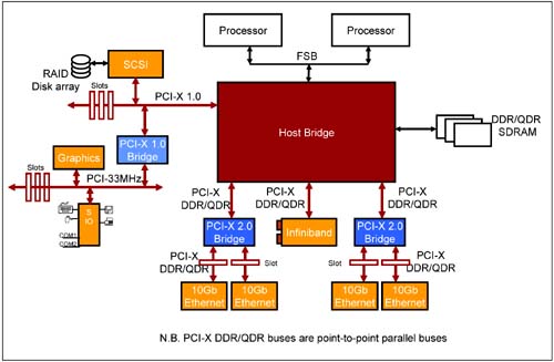
The PCI-X 2.0 specification released in Q1 2002 was designed to further increase the bandwidth capability of PCI-X bus. This bus is described next. DDR and QDR PCI-X 2.0 Bus Based PlatformsFigure 1-19 shows a hypothetical PCI-X 2.0 system. This diagram is the author's best guess as to what a PCI-X 2.0 system will look like. PCI-X 2.0 devices and connectors are 100% hardware and software backwards compatible with PCI-X 1.0 as well as PCI devices and connectors. A PCI-X 2.0 bus supports either Dual Data Rate (DDR) or Quad Data Rate (QDR) data transport using a PCI-X 133 MHz clock and strobes that are phase shifted to provide the necessary clock edges. Figure 1-19. Hypothetical PCI-X 2.0 Bus Based Platform
A design requiring greater than 1 GByte/sec bus bandwidth can implement the DDR or QDR protocol. As indicated in Table 1-2 on page 13, PCI-X 2.0 peak bandwidth capability is 4256 MBytes/sec for a 64-bit 533 MHz effective PCI-X bus. With the aid of a strobe clock, data is transferred two times or four times per 133 MHz clock. PCI-X 2.0 devices also support ECC generation and checking. This allows auto-correction of single bit errors and detection and reporting of multi-bit errors. Error handling is more robust than PCI and PCI-X 1.0 systems making this bus more suited for high-performance, robust, non-stop server applications. Some noteworthy points to remember are that with very fast signal timing, it is only possible to support one connector on the PCI-X 2.0 bus. This implies that a PCI-X 2.0 bus essentially becomes a point-to-point connection with no multi-drop capability as with its predecessor buses. PCI-X 2.0 bridges are essentially switches with one primary bus and one or more downstream secondary buses as shown in Figure 1-19 on page 40. |
| [ Team LiB ] |
|