Transmitter Driver Characteristics
General
Table 12-1 on this page lists the transmitter driver characteristics.
Table 12-1. Output Driver Characteristics|
UI | 400.12 | 399.88 | ps | Unit Interval = the bit time. 400 ps nominal. | TTX-EYE | | 0.7 | UI | Minimum eye width from which maximum jitter can be derived. JT = 1 - TTX-EYE | JT | 0.3 | | UI | Maximum jitter spec shown in Figure 12-11 on page 473. | TTX-RISE
TTX-FALL | | 0.125 | UI | Rise and Fall time for differential signal measured at the 20%/80% voltage point. | VTX-DIFFp-p | 1200 | 800 | mV | Peak-to-peak differential voltage. | VTX-DIFFp | 600 | 400 | mV | Half of VTX-DIFFp-p. | VTX-DC-CM | 3.6 | 0 | V | DC common mode voltage. | VTX-DEEMPH-DIFFp-p-MIN | 566 | 505 | mV | Range of minimum differential peak-to-peak voltages for de-emphasized bits. This is a 3dB - 4dB de-emphasis from pre-emphasized VTX-DIFFp-p-MIN of 800mV. | ITX-SHORT | 90 | | mA | Total current transmitter can provide when shorted to ground. | VTX-IDLE-DIFFp | 20 | 0 | mV | Peak differential voltage under electrical Idle state of Link. | TTX-IDLE-MIN | | 50 | UI | Minimum time a transmitter must be in electrical Idle. | TTX-IDLE-SET-TO-IDLE | 20 | | UI | Time allowed for transmitter to meet electrical Idle transmitter specification after sending electrical Idle Ordered-Set. | TTX-IDLE-TO-DIFF-DATA | 20 | | UI | Maximum time allowed for transmitter to meet differential transmission specification after electrical Idle exit. | ZTX-DIFF-DC | 120 | 80 | Ohms | Transmitter differential mode low impedance. Typical value is 100 Ohms. | ZTX-DC | | 40 | Ohms | Requires minimum D+ and D- line impedance during all power states. | CTX | 200 | 75 | nF | AC coupling capacitor on each Lane placed in close proximity to transmitter. | LTX-SKEW | 1.3 | | ns | Maximum Lane-to-Lane skew at transmitter between any two Lanes. |
Transmit Driver Compliance Test and Measurement Load
The AC timing and voltage parameters shown in Table 12-1 on page 477 is measured within 0.2 inches from the package pins into the test load shown in Figure 12-15.
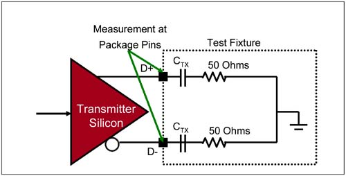
A 50 Ohm probe, or a resistor attached to ground, when attached to the transmit signal pair causes the device to go into the Compliance state of the Link Training and Status State Machine (LTSSM) (see "Polling.Configuration SubState" on page 517). During this state, the device outputs the compliance pattern which can be used for interoperability testing, EMI noise testing, Lane-to-Lane interference testing, Bit Error Rate determination, Transmit and Receive Eye measurements, etc.
|

