Detailed Description of LTSSM States
The subsections that follow provide a description of each of the LTSSM states. Most of the 11 LTSSM states are divided into two or more substates. SubState diagrams are used in the dicussions that follow to illustrate the substates.
Detect State
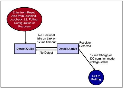
This state is the initial state at power-on time after a Fundamental Reset or after a Hot Reset command generated by the Software Layer. Entry into this state must occur within 80ms of Reset as described in "Reset Exit" on page 496. The Detect state can also be entered from the Disable, Loopback or L2 states. The Detect state is entered if the Configuration, Recovery or Polling states do not complete sucessfully. Figure 14-6 shows the Detect substate machine.
Detect.Quiet SubState
Entry—
From Fundamental Reset or Hot Reset. Also from L2, Loopback, Disable, Polling, Configuration and Recovery states.
During Detect Quiet—
The transmitter is in the Electrical Idle state. The Electrical Idle Ordered-Set does not have to be transmitted before placing the Link in the Electrical Idle state. The transmitter drives a DC common mode voltage (it does not have to meet the 0 - 3.6 V specification). 2.5Gbit/s (Generation 1) transfer rate is initialized (but this is not the rate that will necessarily be advertised via the TS1 and TS2 Ordered-Sets). The Data Link Layer is sent LinkUp = 0.
Exit to Detect.Active—
After 12 ms timeout or when Link exits the Electrical Idle state.
Detect.Active SubState
Entry from Detect.Quiet—
This state is entered after 12ms or when the Link exits the Electrical Idle state.
During Detect.Active—
The transmitter device detects if receivers are connected on all Lanes of the Link. The transmitter starts at a stable DC common mode voltage on all Lanes. This voltage can be VDD, GND, or some other stable voltage in-between. The transmitter then drives a DC common mode voltage other than the one currently presented. A receiver is detected based on the rate at which the D+ and D- lines charge to the new voltage. At design time, the device is designed with knowledge of the charge time to change the voltage (based on the assumed line impedance and transmitter impedance without receiver termination). With a receiver attached at the other end, the charge time will be longer than if there is no connected receiver. For more details on the receiver detection process, see "Receiver Detection" on page 459.
Exit to Detect.Quiet—
Occurs if a receiver is not detected. The loop from Detect.Quiet to Detect.Active is repeated every 12ms, as long as no receiver is attached. The next state is Polling if a Receiver is detected on all unconfigured Lanes.
Exit to Polling—
If the device detects a receiver attached. The Device must now drive a DC common voltage within the 0 - 3.6 V VTX-CM-DC specification.
Special Case—
If all Lanes of a device are not connected to a receiver. For example, a x4 device is connected to a x2 device. In that case, the device detects that some Lanes (two Lanes) are connected to a receiver, while others are not. Those Lanes connected to a receiver belong to one LTSSM.There are two choices at this point: Those Lanes not connected to a receiver belong to another LTSSM (if they can operate as a separate Link—see "Designing Devices with Links that can be Merged" on page 522). The other LTSSM continues to repeat the receiver detection sequence described above. Those Lanes that are not connected to a receiver and cannot become part of another Link and LTSSM must transition the unconnected Lanes to the Electrical Idle state.
Polling State
Introduction
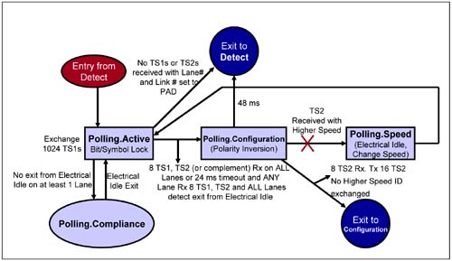
This state is the first time in the Link training and initialization process that PLPs (such as TS1 and TS2 Ordered-Sets) are exchanged between the two connected devices. Figure 14-7 shows the substates of the Polling state machine.
Polling.Active SubState
Entry from Detect—
Transmitters drive a DC common mode voltage within the spec limits on all Lanes on which it detected a receiver.
Entry from Polling.Compliance—
If Electrical Idle exit is detected at the receiver on ALL Lanes that detected a receiver during Detect, the Transmitter exits Polling.Compliance by transmitting 1024 TS1 Ordered-Sets.
Entry from Polling.Speed—
While in Polling.Speed, the Transmitter enters the Electrical Idle state for a minimum of TTX-IDLE-MIN and no longer than 2ms. An Electrical Idle ordered set is sent prior to entering the Electrical Idle state. The DC common mode voltage does not have to be within specification. The Data rate is changed on all Lanes to the highest common data rate supported on both sides of the Link indicated by the training sequence.
During Polling.Active—
- Bit/Symbol Lock are obtained as described in the next bullet (see "Symbol Boundary Sensing (Symbol Lock)" on page 441 and "Achieving Bit Lock" on page 440 for further details). - The transmitters of the two connected devices transmit a minimum of 1024 consecutive TS1 Ordered-Sets on all connected Lanes. The two devices come out of the Detect state at different times, hence the TS1 Ordered-Set exchange of the two devices are not synchronized with one another. The PAD symbol is used in the Lane and Link Numbers fields of the TS1 Ordered-Sets. 1024 TS1 Ordered-Sets amounts to 64µs of time to achieve Bit and Symbol lock.
Exit to Polling.Configuration—
The next state will be Polling.Configuration if one of the following conditions is true: - If a device receives eight consecutive TS1 or TS2 Ordered-Sets (or their complement due to polarity inversion) with Lane and Link set to the PAD symbol on ALL Lanes and at least 1024 TS1 Ordered Sets are transmitted, or - After a 24ms timeout, if: A device receives eight consecutive TS1 or TS2 Ordered-Sets (or their complement) with the Lane and Link numbers set to PAD symbol on ANY Lanes that detected a receiver during Detect, AND at least 1024 TS1 Ordered-Sets were transmitted, AND all Lanes that detected a receiver detected an exit from Electrical Idle at least once since entering Polling.Active (this prevents one or more bad transmitters or receivers from holding up Link configuration).
Exit to Polling.Compliance—
If at least one Lane that detected a receiver during Detect has never detected an exit from Electrical Idle since entering Polling.Active (a passive test load such as a resistor on at least one Lane forces all Lanes into Polling.Compliance).
Exit to Detect—
If no TS1 or TS2 Ordered-Sets are received with the Link and Lane number fields set to the PAD symbol on any Lane. Also, the highest advertised speed must be lowered to generation 1 (if not already advertised as such).
Polling.Configuration SubState
Entry from Polling.Active—
Enters Polling.Configuration if either of the following two conditions are true: - If a device receives eight consecutive TS1 or TS2 Ordered-Sets (or their complement due to polarity inversion) with the Lane and Link numbers set to the PAD symbol on ALL Lanes and at least 1024 TS1 Ordered Sets are transmitted, or - After a 24ms timeout, if a device receives eight consecutive TS1 or TS2 Ordered-Sets (or their complement) with the Lane and Link numbers set to the PAD symbol on ANY Lanes that detected a receiver while in the Detect state, and at least 1024 TS1 Ordered-Sets were transmitted, AND all Lanes that detected a receiver detected an exit from Electrical Idle at least once since entering Polling.Active (prevents one or more bad transmitters or receivers from holding up Link configuration).
During Polling.Configuration—
- If a receiver sees the complement of the TS1/TS2 Ordered-Sets, it has to invert the polarity of its differential input pair terminals. Basically, if D21.5 rather than D10.2 is received in the TS1 Ordered-Set, or if D26.5 rather than D5.2 is received for the TS2 Ordered-Set, then the receiver (not the transmitter) must invert its signal polarity. Polarity Inversion is a mandatory feature (see "Link Initialization and Training Overview" on page 500 for example of Polarity Inversion) and must be implemented on all Lanes independently. - The Transmitter sends more than eight TS2 Ordered-Sets.
Exit to Configuration—
Assumes that no speed > 2.5Gbits/s is identified in the Data Rate Identifier field of the TS2 Ordered-Set. After receiving eight consecutive TS2 Ordered-Sets and transmitting 16 TS2 Ordered-Sets after receiving one TS2 Ordered-Set, exit to Configuration.
Exit to Polling.Speed—
The next state is Polling.Speed after eight consecutive TS2 Ordered Sets, with Link and Lane numbers set to the PAD symbol (K23.7), are received on any Lanes that detected a Receiver during Detect, 16 TS2 Ordered Sets are transmitted after receiving one TS2 ordered set, and at least one of those same Lanes is transmitting and receiving a Data Rate Identifier greater than 2.5Gb/s.
Exit to Detect—
If neither of the two exit conditions are met, exit to Detect after a 48ms timeout.
Polling.Compliance SubState
Entry from Polling.Active—
The next substate is Polling.Compliance if at least one Lane that detected a receiver during Detect has never detected an exit from the Electrical Idle state on its receiver since entering Polling.Active (a passive test load, such as a resistor, on at lease one Lane forces all Lanes into Polling.Compliance).
During Polling.Compliance—
A test probe (of 50 Ohms impedance) or a 50 Ohm impedance to ground hooked to the transmit pair on any Lane causes the device to enter Polling.Compliance (see "Transmit Driver Compliance Test and Measurement Load" on page 479"). In this state, the device (a pattern generator) is required to generate the compliance pattern on the Link. The compliance pattern selected produces the worst case interference between neighboring Lanes and results in the worst case EMI . Test equipment hooked to the Link is used to test for EMI noise, cross-talk, Bit Error Rate (BER), etc. - The Transmitter outputs the compliance pattern on all Lanes that detected a receiver during Detect. The pattern consists of the 8b/10b symbols K28.5, D21.5, K28.5, and D10.2. Current running disparity (CRD) must be set to negative before sending the first symbol. - No Skip Ordered-Sets are transmitted during Polling.Compliance.
Polling.Compliance Exit—
The compliance state is exited when an Electrical Idle exit is detected on all the Lanes that detected a receiver during Detect. The transmitter exits Polling.Compliance by transmitting 1024 TS1 Ordered-Sets.
Polling.Speed SubState
Entry from Polling.Configuration—
Polling.Speed is entered if: - Eight consecutive TS2 Ordered-Sets are received, and - 16 TS2 Ordered-Sets are transmitted after receiving one TS2, and - at least one of the Lanes is transmitting and receiving with a Data Rate Identifier in the TS2 Ordered-Set that is higher than 2.5Gb/s.
During Polling.Speed—
In this state, the transmitter enters the Electrical Idle state for at least 50 UI (20ns), but no longer than 2ms. An Electrical Idle Ordered-Set is sent prior to entering the Electrical Idle state and the DC common mode voltage (VTX-CM-DC) does not have to be within the specified tolerance. During this state, the data rate is changed on all Lanes to the highest common data rate supported by both ends of the Link.
Exit to Polling.Active—
This is the default.
Configuration State
General
The main function of this state is the assignment of Link numbers and Lane numbers to each Link that is connected to a different device. The Link is also De-skewed in this state.
An upstream device sends TS1 Ordered-Sets on all downstream Lanes. This starts the Link numbering and Lane numbering process. If the width determination and Lane numbering is completed successfully, then TS2 Ordered-Sets are transmitted to the neighboring device to confirm the Link Width, Link Number and Lane Number for each Link connected to a different device.
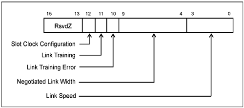
While in the Configuration state, the Link Training bit in the Link Status register is set by hardware (see Figure 14-22 on page 552). This bit is set on Root Complex ports and on downstream Switch ports. It is not set in Endpoints or a Switch upstream ports.
Configuration.RcvrCfg SubState
Entry from Polling or Recovery—
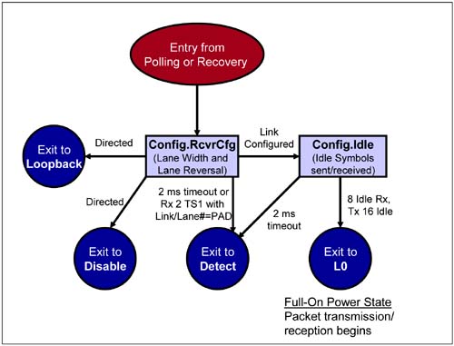
This state is entered after the normal completion of the Polling state (as described in "Polling.Configuration SubState" on page 517). It is also entered if the Recovery state fails to complete successfully (as described in"Recovery State" on page 532).
During Configuration.RcvrCfg—
- The Link Number of each Link connected to a unique device is negotiated. - The Lanes of each unique Link are numbered starting with Lane 0. If necessary, the Lane Numbers are reversed. - Those Lanes that are not part of a new Link are disabled and enter the Electrical Idle state. Disabled Lanes are re-enabled if the device enters the Detect state again. - Each device advertises its N_FTS value in the TS1/TS2 Ordered-Sets it sends to the remote device. - A receiver uses the COM symbol in the received TS1 and TS2 Ordered-Sets to de-skew the Lanes of the Link (see "Lane-to-Lane De-Skew" on page 444).
Rather than go through a tedious process to explain the Configuration.RcvrCfg function, three examples are presented in "Examples That Demonstrate Configuration.RcvrCfg Function" on page 524. That section describes the Link Numbering and Lane Numbering procedure.
Exit to Configuration.Idle—
When the Link Numbering and Lane Numbering process has completed successfully.
Exit to Detect—
The next state is Detect if, after a 2ms timeout, no Link or Lanes could be configured, or if all Lanes receive two consecutive TS1 Ordered-Sets with the Link and Lane Number fields set to the PAD symbol.
Exit to Disable or Loopback—
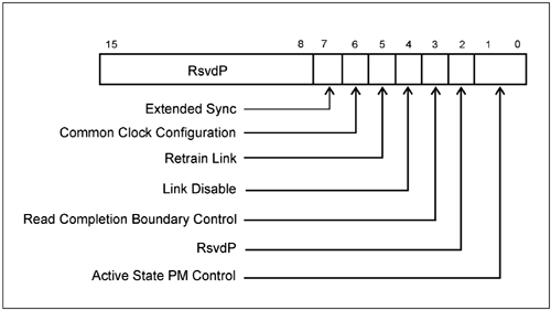
If directed to enter the Disable or Loopback state by higher layers: - Software can inform a Loopback Master connected to the Link to enter the Loopback state in an implementation specific manner. The Loopback Master device continuously sends TS1 Ordered-Sets to the Loopback Slave with the Loopback bit set in the TS1 Training Control field until the Loopback slave returns TS1 Ordered-Sets with the Loopback bit set. The Loopback Slave enters Loopback when it receives two consecutive TS1 Ordered-Sets with the Loopback bit set. - Similarly, software can command a device to enter the Disable state by setting the Disable bit in the Link Control register (see Figure 14-23 on page 553). This device (a downstream port) then transmits 16 TS1 Ordered-Sets with the Disable Link bit set in the TS1 Training Control field. A connected receiver (on an upstream port) is disabled when it receives TS1 Ordered-Sets with the Disable Link bit set.
Configuration.Idle SubState
Entry from Configuration.RcvrCfg—
When the Link Numbering and Lane Numbering process has completed successfully.
During Configuration.Idle—
The Link is fully configured. Bit Lock and Symbol Lock have been achieved. The Link data rate has been selected. The Link and Lane Numbers have been assigned. - The Transmitter sends Logical Idle sequences (see "Logical Idle Sequence" on page 436) on all configured Lanes. At least 16 Logical Idle sequences are sent. - The Receiver waits for the receipt of the Logical Idle data. - The receivers Data Link Layer LinkUp status bit is set to 1.
Exit to L0—
Occurs when eight Logical Idle symbols are received on all configured Lanes and 16 Logical Idles are sent after receiving 1 Logical Idle. L0 is the full-on power state during which normal packet transmission and reception can occur. The differential transmitters and receivers are enabled in the low impedance state.
Exit to Detect—
Occurs when, after a 2ms timeout, no Logical Idle symbols have been exchanged.
Designing Devices with Links that can be Merged
General
A designer decides how many Lanes to implement on a given Link based on performance requirements for that Link. The specification requires that a device that implements a multi-Lane Link must be designed to operate as a one-x1 Link also. This allows such a multi-Lane Link device to operate when and if it connects to a x1 Link device (Link performance is lower, however).
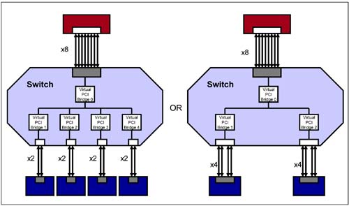
An optional feature allows two or more downstream Links (associated with different ports) of a switch to be combined to form a wider Link that is connected to one device. Figure 14-9 on page 524 shows a Switch with one upstream port and four downstream ports. The Switch supports eight upstream Lanes and eight downstream Lanes. On the downstream side, the Switch supports four ports. It is therefore four-x2 capable. By combining two ports, it is also two-x4 capable. As required by the specification, each port must be x1 capable.
Four-x2 Configuration
The Switch is capable of supporting up to four downstream ports, with each port a x2 port (four-x2 capable on the downstream side) that connects to four devices (left side of Figure 14-9 on page 524). The bridge internally consists of one upstream logical bridge and four downstream logical bridges.
During Link Training, while in the Configuration.RcvrCfg substate, the LTSSM of each switch downstream port establishes that it is connected to four devices with x2 Links each. Essentially, the switch consists of four ports, four LTSSMs, four Physical Layers, four Data Link Layers and four Transaction Layers.
Two-x4 Configuration
This switch design also allows its downstream Lanes to be combined into two downstream x4 ports (right side of Figure 14-9). In other words, the eight downstream Lanes may be wired to two, independent x4 devices. In thise case, the switch consists of one upstream logical bridge and two downstream logical bridges.
During Link Training, while in the Configuration.RcvrCfg substate, the LTSSM of each switch downstream port establishes that it is connected to two downstream devices with x4 Links each. Essentially, the switch in this configuration has two downstream ports and the four switch LTSSMs are merged into two LTSSMs. The switch has two Physical Layers, two Data Link Layers and two Transaction Layers on the downstream side.
The switch is capable of four-x2 Links on the downstream side (left) or two-x4 Links (right), depending on how the designer chooses to wire up the downstream switch Lanes.
During the Configuration.RcvrCfg state, the LTSSM discovers how the downstream Lanes are wired. Each Link that connects to a unique device is numbered uniquely and each Lane of a Link is also numbered. Designing a switch with this capability is no trivial task, so the feature that permits the combining or splitting of Links to form a wider or narrower Link is optional.
It is a requirement that each multi-Lane port be able to operate as a x1 port when connected to a x1 device.
Examples That Demonstrate Configuration.RcvrCfg Function
The Link numbering and Lane numbering process is initiated by an upstream device during the Configuration.RcvrCfg substate. A Root Complex or a Switch downstream port would initiate the Configuration.RcvrCfg process. Endpoints and upstream ports are downstream devices and do not initiate this process.
TS1 and TS2 Ordered-Sets are transmitted and received during this substate. Upon exit from the Configuration.RcvrCfg substate, each Link has been initialized with a Link number (this indirectly establishes the number of ports a device supports). Each Lane has also been initialized with a Lane number (this indirectly establishes the Link width).
Three examples are covered in the next three sections.
RcvrCfg Example 1
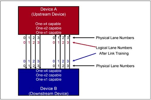
Consider Figure 14-10 on page 527. Device A is one-x4 capable, one-x2 capable and one-x1 capable (One-x1 support is required by the spec). Device B is one-x4 capable, one-x2 capable and one-x1 capable (it is required to support this capability by the spec). The device pins associated with each Lane are physically numbered 0, 1, 2 and 3 (shown in the Figure 14-10), though the assigned Logical Lane numbers may have been changed while in Configuration.RcvrCfg substate (in this example, the Logical Lane Number remains the same as the physical Lane Number).
Link Number Negotiation
Mechanism:
Upstream Device A transmits TS1 Ordered-Sets with the Link Number for each group of connected Lanes set to a device-specific initial value. As an example, a switch with four downstream ports may initially set the Link numbers to 0, 1, 2, and 3. The Lane Number field is initially set to the PAD symbol (K23.7). Actions Taken:
This implies that Device A sends four TS1 Ordered-Sets on the four Lanes. The four TS1 Ordered-Sets each contain a Link Number n, n, n, n, and the Lane Number fields are set to the PAD symbol. Even though Device A is also capable of One-x1 and One-x2 operation, Device A starts by assuming the capability that maximizes the use of all connected Lanes.
Mechanism:
Downstream Device B returns TS1 Ordered-Sets on all connected Lanes that received TS1 Ordered-Sets with the assigned common Link Number for Lanes it can support as one Link. The Lane Numbers are initailly set to the PAD symbol (K23.7). Actions Taken:
Device B returns a TS1 Ordered-Set on all four Lanes. The TS1 Ordered-Sets on each Lane contains Link Number n. The Lane Number field contains the PAD symbol. Device A sees the TS1 Ordered-Set with Link numbers of n on each Lane. Device A establishes that its four Lanes are connected to one downstream device and that the Link is numbered as n. Device A has received confirmation from Device B that its Link can be numbered n, where n is a number between 0 and 255. The Link is configured as a One-x4 Link.
The Link Number of n is a logical Link Number that is not stored in a defined configuration register. This number is hard-wired by design, and not related to the Port Number field of the Link Capability Register.
Also, the Negotiated Link Width field in the Link Status register of both the upstream and downstream devices are updated with "000100", indicating a x4 Link (see Figure 14-22 on page 552).
Lane Number Negotiation
Mechanism:
Upstream Device A sends TS1 Ordered-Sets on all connected Lanes with the configured Link Number and unique Lane Numbers starting with 0 for each Lane. PAD symbols are no longer sent in the Lane Number field. Actions Taken:
Device A sends four TS1 Ordered-Sets with Link Number of n and Lane Numbers of 0, 1, 2 and 3, respectively, on each connected Lane.
Mechanism:
Downstream Device B returns TS1 Ordered-Sets on all connected Lanes with the same Link Number as contained in the received TS1 Ordered-Sets and the same Lane Numbers for each Lane as indicated in the received TS1 Ordered-Sets. If the downstream device's Lanes are hooked in the reverse manner and it does not support the Lane Reversal feature, it returns the TS1 Ordered-Sets with the Lane Number field indicating the manner in which it wants the Lanes to be numbered. Hopefully, the upstream device supports Lane Reversal and accepts the reverse order in which the downstream device wants the Lanes numbered. Actions Taken:
Device B returns four TS1 Ordered-Sets with a Link Number of n and Lane Numbers of 0, 1, 2 and 3, respectively, on each connected Lane.
Confirmation of Link Number and Lane Number Negotiated
Step 5 and 6. Mechanism:
Device A and B confirm the Link Number and Lane Numbers negotiated by exchanging TS2 Ordered-Sets. Actions Taken:
Device A and B exchange TS2 Ordered-Sets with the Link Number set to n and the Lane Numbers set to 0, 1, 2 and 3, respectively, for each of the four Lanes. In this example, the Logical Lane Numbers of both devices remain the same as the physical Lane Numbers.
RcvrCfg Example 2
Consider Figure 14-11 on page 529. This is an example in which upstream device A is capable of one-x4, or two-x2, or two-x1. The narrowest Link capability that uses ALL Lanes is two-x2. The two ports of Device A are each x2 capable and the physical Pin Number (Lane number) of each port is 0 and 1. Device B and C each have one port that is x2 capable and the physical Pin Number (Lane number) of each port is 0 and 1.
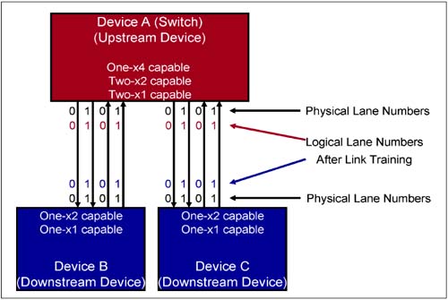
Using a strapping option on Device A (or by default), it starts the Configuration.RcvrCfg substate by reporting its two-x2 capability when transmitting TS1 Ordered-Sets to the downstream devices.
Link Number Negotiation
Mechanism:
Upstream Device A transmits TS1 Ordered-Sets with an assumed Link Number value for each group of Lanes capable of acting as unique Links. For now, the Lane Number is set to the PAD symbol (K23.7) Actions Taken:
Device A sends TS1 Ordered-Sets on all four Lanes. The TS1 Ordered-Set on each Lane contains Link number n, n, n+1, and n+1. The Lane Number field contains the PAD symbol.
Mechanism:
Downstream Devices B and C return TS1 Ordered-Sets containing the Link number for Lanes it can support as one Link. The Lane Number is initially set to the PAD symbol (K23.7). Actions Taken:
Device B and C return TS1 Ordered-Sets on each Lane, each containing a Link Number of n for Device B and a Link Number of n+1 for Device C. The Lane Number field is initially set to the PAD symbol. Device A receives TS1 Ordered-Sets on two of the Lanes with a Link Number of n and TS1 Ordered-Sets on the other two Lanes with a Link Number of n+1.
The Link Number of n and n+1 is a logical Link Number that is not stored in a defined configuration register. This number is not related to the Port Number field of the Link Capability Register of upstream Device A's port or Device B's or Device C's port.
Also, the Negotiated Link Width field in the Link Status register of both upstream ports and downstream ports are updated with "000010," indicating a x2 Link (see Figure 14-22 on page 552).
Lane Number Negotiation
Mechanism:
Device A realizes that its Lanes are divided into two Links and sends TS1 Ordered-Sets on all connected Lanes with Link Number n on two Lanes and Link Number n+1 on the other two Lanes. PAD symbols are no longer sent in the Lane Number field. Actions Taken:
Device A sends a TS1 Ordered-Set on two Lanes with a Link Number of n in both of the TS1s, a Lane Number of 0 in one of the TS1s, and a Lane Number of 1 in the other TS1. Device A also sends a TS1 on each of the other two Lanes with a Link Number of n+1 in both of the TS1s, a Lane Number of 0 in one TS1, and a Lane Number of 1 in the other TS1.
Mechanism:
Downstream Device B and C returns TS1s on all connected Lanes with the same Link Number as contained in the received TS1 Ordered-Sets and the same Lane Numbers for each Lane as in the received TS1 Ordered-Sets. If the downstream devices' Lanes are hooked in the reverse manner and they do not support the Lane Reversal feature, they return the TS1 Ordered-Sets with the Lane Number fields reversed. Hopefully, the upstream device supports Lane Reversal and accepts the reverse order that the downstream devices want the Lanes numbered. Actions Taken:
Device B returns TS1s on each Lane with Link Number of n and a Lane Number of 0 in one TS1 Ordered-Set and a Lane Number of 1 in the other. Device C returns a TS1 on each Lane with a Link Number of n+1 and a Lane Number of 0 in one TS1 Ordered-Set and a Lane Number of 1 in the other.
Confirmation of Link Number and Lane Number Negotiated
Step 5 and 6 Mechanism:
Device A and B/C confirm the Link Numbers and Lane Numbers negotiated by exchanging TS2 Ordered-Sets. Actions Taken:
Device A and B exchange a TS2 Ordered-Set on each Lane with the Link Number set to n and the Lane Numbers set to 0 and 1, respectively, for each of the two Lanes on the first Link. Device A and C exchange a TS2 Ordered-Set on each Lane with the Link Number set to n+1 and the Lane Numbers set to 0 and 1, respectively, for each of the two Lanes of the second Link. Each Lane of the two Links in this example are logically numbered 0 and 1, matching the physical Pin number (Lane number) of each Lane.
RcvrCfg Example 3
Consider Figure 14-12 on page 532. This is an example in which upstream device A is capable of one-x4, or two-x2, or two-x1 (the same as Device A in the previous example). The narrowest Link capability that uses ALL Lanes is two-x2. Each Lane of Device A's two ports are physically numbered 0 and 1.
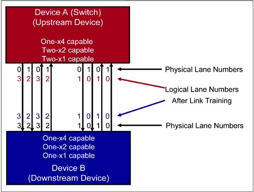
Via a strapping option on Device A (or by default), it reports its two-x2 capability when transmitting TS1 Ordered-Sets to the downstream device. In this example, Device A initially assumes that it has two-x2 downstream Links. Also, both of Device A's Links are connected to downstream Device B. Device B is x4 capable. Its pins (or Lanes) are physically numbered 3, 2, 1, 0, respectively. In this example, assume that Device B does not support Lane Reversal, but Device A does support Lane Reversal.
Link Number Negotiation
Mechanism:
Upstream Device A transmits TS1 Ordered-Sets with an assumed Link Number field for each group of Lanes capable of being unique Links that use up all the Lanes. For now, the Lane Number is set to the PAD symbol (K23.7). Actions Taken:
Device A sends four TS1 Ordered-Sets on the four Lanes. Each TS1 Ordered-Set contains the respective Link number (n, n, n+1, n+1). The Lane Number field is initially set to the PAD symbol.
Mechanism:
Downstream Device B returns TS1 Ordered-Sets with an assigned common Link number for Lanes it can support as one Link. The Lane Number is initially set to the PAD symbol (K23.7). Actions Taken:
Device B returns TS1 Ordered-Sets on each Lane, each containing a Link Number of n. The Lane Number field is initially set to the PAD symbol. Device A sees TS1 Ordered-Sets on four Lanes with a Link Number of n, telling Device A that its four Lanes are connected to one downstream device and that the Link should be numbered n.
The Link Number of n is a logical Link Number that is not stored in a defined configuration register. This number is not related to the Port Number field of the Link Capability Register.
Also, the Negotiated Link Width field in the Link Status register of both the upstream port and the downstream port are updated with "000100", indicating a x4 Link (see Figure 14-22 on page 552).
Lane Number Negotiation
Mechanism:
Device A realizes that its four Lanes are combined into one Link (One-x4) and sends TS1 Ordered-Sets on all connected Lanes with one assumed Link Number, n, and a unique Lane Number is assigned to each Lane of the Link. PAD symbols are no longer sent in the Lane Number field. Actions Taken:
Device A sends TS1 Ordered-Sets on four Lanes with a Link Number of n and Lane Numbers 0, 1, 2, and 3, respectively, numbered left to right.
Mechanism:
Downstream Device B returns a TS1 on all connected Lanes with the same Link Number n as contained in the received TS1 Ordered-Set. Assume that the Lanes are hooked up in reverse manner as shown in Figure 14-12 on page 532 and that Device B does not support the Lane Reversal feature. If the downstream device's Lanes are reversed and it does not support Lane Reversal, it returns the TS1 Ordered-Sets with the Lane Number fields reversed. Hopefully, the upstream device supports Lane Reversal and accepts the reverse ordering of the Lanes. Actions Taken:
Device B returns a TS1 Ordered-Set on each Lane with a Link Number of n and Lane Numbers of 3, 2, 1 and 0, respectively, numbered from left to right.
Confirmation of Link Number and Lane Number Negotiated
Step 5 and 6 Mechanism:
Device A and B confirm the Link Number and the Lane Numbers negotiated by exchanging of TS2 Ordered-Sets. Actions Taken:
Device A and B exchange a TS2 Ordered-Set on each Lane with the Link Number set to n and the Lane Numbers set to 3, 2, 1 and 0 (Lanes reversed), respectively, for each of the four Lanes.
Device A's physical Pin Numbers (Lane numbers) for the four Lanes from left to right are 0, 1, and 0, 1 (the same numbers repeated—because Device A is two-x2 port capable). However, Device A ends up with logical Lane Numbers of 3, 2, 1, 0, from left to right. Device B's physical Pin Numbers are 3, 2, 1 and 0, from left to right. The logical Lane Numbers remain the same as the physical Lane Numbers: 3, 2, 1 and 0.
Consider what would happen if Device A did not support Lane Reversal (Lane Reversal is an optional feature). In Step 4, Device B returns four TS1 Ordered-Sets with Lane Numbers of 3, 2, 1 and 0. Device A would not be able to reverse the physical Lane numbers of 0, 1, 2 and 3 that it proposed in Step 3. The Link training process freezes at this point. This is a Link training error and is reported by the upstream device (Device A) via the Link Training Error bit in the Link Status register (see Figure 14-22 on page 552). A system designer would be wrong to hook the Lanes of two devices that do not support Lane Reversal in a reversed manner.
Recovery State
The Recovery state is also referred to as the Re-Training state. It is not entered during Link training (which occurs when a device comes out of reset). The Recovery state is entered when a receiver needs to regain Bit and Symbol Lock, or if an error occurs while in L0 that renders the Link inoperable. Rather than going through the Polling and Configuration states (which have longer latencies associated with them), the Recovery state has a much shorter latency (the PLLs are already operational and may only need to be sync'd). The number of FTS Ordered-Sets (N_FTS) required for L0s exit is re-established in Recovery and the Link is de-skewed. The Link Number, Lane Numbers and bit transfer rate (2.5Gbits/s) remain unchanged. If any of these three variables have changed since the time the link was in the Configuration state, the LTSSM transitions from the Recovery state to the Configuration state.
Reasons that a Device Enters the Recovery State
Exit from L1 (requires that the receiver be re-trained). Exit from L0s when the receiver is unable to achieve Bit/Symbol Lock due to the reception of an insufficient number of FTS Ordered-Sets. In case of an error that renders the Link unreliable, software sets the Retrain Link bit in the Link Control Register (see Figure 14-23 on page 553). An error condition that occurs in the L0 state that renders the Link unreliable may automatically cause the Data Link Layer or Physical Layer logic to initiate a re-train cycle. Reception of TS1 or TS2 Ordered-Sets on any configured Lane from a remote transmitter signals the receiver to retrain the link. A receiver detects that the Link has transitioned to the Electrical Idle state on all configured Lanes without first receiving the Electrical Idle Ordered-Sets from the transmitter.
Initiating the Recovery Process
Both devices on a Link go through Recovery together. One of the two devices initiates the Recovery process, transmitting TS1 Ordered-Sets to its neighbor. The neighbor goes through Recovery and returns the favor by returning TS1 Ordered-Sets that the initiator's receiver uses to go through Recovery. In transmitting and receiving TS1 Ordered-Sets, both the receiver and the transmitter of the Ordered-Sets regains Bit/Symbol Lock, and then returns to the L0 state.
Refer to Figure 14-13 on page 537 for the detailed steps involved in completing the Recovery process described below.
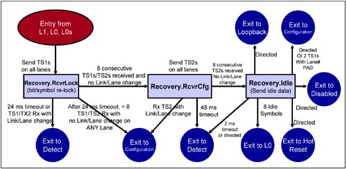
Recovery.RcvrLock SubState
Entry from L0—
A device enters Recovery for the reasons sited in "Reasons that a Device Enters the Recovery State" on page 533.
Entry from L1—
The Receiver detects Electrical Idle exit, or when directed by higher-level software. Electrical Idle exit means that the receiver detected a valid differential voltage and starts seeing TS1 Ordered-Sets.
Entry from L0s—
The Receiver enters into Recovery when it detects an N_FTS timeout (i.e., if the receiver is unable to re-obtain Bit/Symbol Lock after receiving N_FTS FTS Ordered-Sets, or if it receives an insufficient number of FTS Ordered-Sets, then instead of going to L0, it goes to Recovery).
During Recovery.RcvrLock—
- The transmitter sends TS1 Ordered-Sets on all configured Lanes (with the same Link and Lane Numbers as set during the Configuration state). The specification is unclear about how many TS1 Ordered-Sets the transmitter should send, but the author ventures to guess that it should send TS1 Ordered-Sets until this substate is exited. - If the Extended Sync bit is set by software in the Link Control register (see Figure 14-23 on page 553), the transmitter must send a minimum of 1024 TS1 Ordered-Sets to allow an external monitoring device (i.e., a tool), if connected, to sync (obtain Bit/Symbol Lock). - The receiver uses the received TS1 Ordered-Sets to obtain Bit/Symbol Lock. - A device advertises its N_FTS value via the TS1 Ordered-Sets it sends to the remote device. This number can change from what it was during the Configuration state. - A receiver uses the COM symbol in the received TS1 and TS2 Ordered-Sets to de-skew the Lanes of the Link (see "Lane-to-Lane De-Skew" on page 444).
Exit to Recovery.RcvrCfg—
A receiver moves to Recover.RcvrCfg if eight consecutive TS1 or TS2 Ordered-Sets are received without Link and Lane Number changes.
Exit to Configuration—
After 24ms, if the receiver detects at least one TS1 (but not eight consecutive TS1 Ordered-Sets) on ANY configured Lanes and the Link Number and Lane Number are the same as the numbers Transmitted in the TS1 Ordered-Sets, then it exits to Configuration.
Exit to Detect—
After a 24ms timeout, if the receiver does not detect TS1 or TS2 Ordered-Sets, or it detects TS1 or TS2 Ordered-Sets with the Link or Lane Number different from the numbers in the transmitted TS1 or TS2 Ordered-Sets, then it exits to Detect.
Recovery.RcvrCfg SubState
Entry from Recovery.RcvrLock—
A receiver moves to Recover.RcvrCfg if eight consecutive TS1 or TS2 Ordered-Sets are received without Link and Lane Number changes.
During Recovery.RcvrCfg—
- The Transmitter sends TS2s on all configured Lanes (with the same Link and Lane Numbers configured earlier). Again, the specification is unclear about how many TS2 Ordered-Sets the transmitter should send, but the author ventures to guess that it should send TS2 Ordered-Sets until this substate is exited. - If the N_FTS value changes, the device must note the new value. - If the Link was not de-skewed in the Recovery.RcvrLock substate, a receiver uses the COM symbol in the received TS1 and TS2 Ordered-Sets to de-skew the Lanes of the Link (see "Lane-to-Lane De-Skew" on page 444).
Exit to Recovery.Idle—
If eight consecutive TS2 Ordered-Sets are received with no Link/Lane Number changes and 16 TS2 Ordered-Sets are sent after receiving one TS1 or TS2 Ordered-Set, then exit to Recovery.Idle.
Exit to Configuration—
If eight consecutive TS1 Ordered-Sets are received on ANY Lane with Link or Lane Numbers that do not match what is being transmitted, then exit to Configuration state.
Exit to Detect—
Exit to Detect after a 48ms timeout and the state machine has not exited to Recovery.Idle or Configuration state.
Recovery.Idle SubState
Entry from Recovery.RcvrCfg—
Enter from Recovery.RcvrCfg if eight consecutive TS2 Ordered-Sets are received with no Link/Lane Number changes and 16 TS2 Ordered-Sets are sent after receiving one TS1 or TS2 Ordered-Set.
During Recovery.Idle—
- The Transmitter sends Logical Idle symbols on all configured Lanes unless exiting to Disable, Hot Reset, Configuration, or Loopback. - The Receiver waits for the receipt of Logical Idle symbols on all Lanes.
Exit to Disable, Loopback or Hot Reset—
If directed by higher layers to enter the Disable, Loopback or Hot Reset state. The device transmits TS1 or TS2 (TS2 not valid for Hot Reset case) with the Disable, Loopback or Hot Reset bits set. If a device receives two consecutive TS1s or TS2s (TS2 not valid for Hot Reset case) with the Disable, Loopback or Hot Reset bit set, it exits to the Disable, Loopback or Hot Reset state respectively. Software can inform a Loopback Master connected to the Link to enter the Loopback state using an implementation specific mechanism. The Loopback Master device continuously sends TS1 Ordered-Sets to the Loopback Slave with the Loopback bit set in the TS1 Training Control field until the Loopback slave returns TS1 Ordered-Sets with the Loopback bit set. The Loopback Slave enters Loopback when it receives two consecutive TS1s with the Loopback bit set. Similarly, software can command a device to enter the Disable state by setting the Disable bit in the Link Control register (see Figure 14-23 on page 553). This device (a downstream port) then transmits 16 TS1 Ordered-Sets with the Disable Link bit set in the TS1 Training Control field. A connected receiver (on the upstream port) is disabled when it receives a TS1 with the Disable Link bit set. Similarly, software can command a device to enter the Hot Reset state by setting the Secondary Bus Reset bit in the Bridge Control register (see "In-Band Reset or Hot Reset" on page 491). This device (a downstream port) then transmits TS1 Ordered-Sets continuously for 2ms with the Hot Reset bit set in the TS1 Training Control field. A receiver (in the upstream port) detects the Hot Reset when it receives at least two TS1 Ordered-Sets with the Hot Reset bit set.
Exit to Configuration—
Exits to the Configuration state if directed by a higher layer to re-configure the link, or if two consecutive TS1s are received with Lane numbers set to the PAD symbol.
Exit to L0—
If eight Logical Idle symbols are received on all configured Lanes.
Exit to Detect—
Exit to Detect after a 2ms timeout if the LTSSM does not exit to any of the other states above.
L0 State
Enter from Configuration—
This state is entered from Configuration.Idle substate if eight Logical Idle symbols are received on all configured Lanes and 16 Logical Idles are sent after receiving one Logical Idle.
Enter from Recovery—
This state is entered from the Recovery.Idle substate if eight Logical Idle symbols are received on all configured Lanes.
Enter from L0s—
This state is entered from L0s if a device receives the appropriate number of FTS Ordered-Sets and re-obtains Bit and Symbol Lock.
During L0—
- This is the fully-operational Link state during which TLP, DLLP and PLP transmission and reception can occur. - The differential transmitters and receivers are enabled in the low impedance state. - LinkUp=1
Exit to Recovery—
A device enters Recovery for any of the reasons sited in "Reasons that a Device Enters the Recovery State" on page 533.
Exit to L0s—
The Transmitter enters L0s when directed to do so by its higher layers. A Receiver enters L0s when it receives an Electrical Idle Ordered-Set and the Link transitions to the Electrical Idle state.
Exit to L1—
See "L1 State" on page 541 for a detailed description.
Exit to L2—
See "L2 State" on page 543 for a detailed description.
L0s State
This is a lower power state that has the shortest exit latency to L0. Devices manage entry and exit from this state automatically without any higher level software involvement.
L0s Transmitter State Machine
Figure 14-14 on page 539 shows the transmitter state machine associated with L0s state entry and exit.
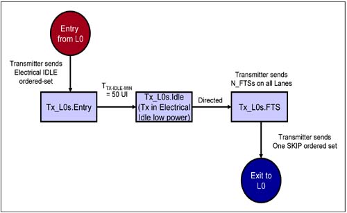
Tx_L0s.Entry SubState
Entry from L0—
The L0s state machine is entered when the device is directed to do so by an upper layer. This may occur via a timeout mechanism triggered due to periods of inactivity (no TLP, DLLP or PLP transmission activity) on the Link.
During Tx_L0s.Entry—
- The Transmitter sends an Electrical Idle Ordered-Set and the Link enters the Electrical Idle state. - The Transmitter drives a DC common mode voltage between 0 - 3.6 V.
Exit to Tx_L0s.Idle—
Exit to Tx_L0s.Idle after 50 UI (20ns) while the transmitter drives a stable DC common mode voltage.
Tx_L0s.Idle SubState
Entry from Tx_L0s.Entry—
Enter Tx_L0s.Idle after 50 UI (20 ns) while the transmitter drives a stable DC common mode voltage.
During Tx_L0s.Idle—
- The Link is in the Electrical Idle state. - The transmitter's output impedance could be low or high.
Exit to Tx_L0s.FTS—
Exit to Tx_L0s.FTS if directed to do so by a higher layer. For example, when it is time for a device to resume packet transmission, it will exit this state.
Tx_L0s.FTS SubState
Entry from Tx_L0s.Idle—
Enter Tx_L0s.FTS if directed to do so by a higher layer.
During Tx_L0s.FTS—
- To exit the Electrical Idle substate, the transmitter sends the number of FTS Ordered-Sets specified by N_FTS. The N_FTS number is defined during Link Training (Configuration and Recovery states) during which each device advertises the number of FTS sets it requires to achieve lock. - If the Extended Synch bit is set (see Figure 14-23 on page 553), the transmitter sends 4096 FTS Ordered-Sets instead of N_FTS number of FTS Ordered-Sets. - Follow this by one Skip Ordered-Set. No SKIP Ordered-Sets are transmitted during the transmission of FTS Ordered-Sets.
Exit to L0—
Exit to L0 state after the Skip Ordered-Set transmission.
L0s Receiver State Machine
Figure 14-15 on page 541 shows the receiver state machine associated with L0s state entry and exit.
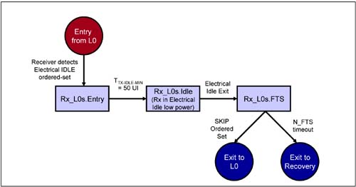
Rx_L0s.Entry SubState
Entry from L0—
This lower power state is entered if a receiver receives an Electrical Idle Ordered-Set.
During Rx_L0s.Entry—
- Wait in the state for minimum of 50 UI (20ns). - The receiver's input impedance remains low.
Exit to Rx_L0s.Idle—
Exit to Rx_L0s.Idle after 50 UI (20ns).
Rx_L0s.Idle SubState
Entry from Rx_L0s.Entry—
Enter Rx_L0s.Idle after 50 UI (20ns).
During Rx_L0s.Idle—
Wait until the receiver detects an Electrical Idle exit (i.e., a valid differential voltage is seen on the receivers).
Exit to Rx_L0s.FTS—
The next state is Rx_L0s.FTS if the receiver detects Electrical Idle exit on any configured Lane.
Rx_L0s.FTS SubState
Entry from Rx_L0s.Idle—
Enter this state from Rx_L0s.Idle if the receiver detects Electrical Idle exit on any configured Lane.
During Rx_L0s.FTS—
- Receiver obtains Bit/Symbol Lock if a sufficient number of FTS Ordered-Sets are received. - The receiver must be able to receive packets after this state.
Exit to L0—
Exit to L0 state after Skip Ordered-Set reception and a sufficient number of FTS Ordered-Sets are received (as advertised during the Configuration or Recovery states via the N_FTS field of the TS1/TS2 Ordered-Set).
Exit to Recovery—
Recovery state is entered if an N_FTS timeout occurs (i.e., if the receiver receives an insufficient FTS Ordered-Sets to re-obtain Bit/Symbol Lock).
L1 State
This is a lower power state than L0s and has a longer exit latency than the L0s exit latency. Devices can manage entry and exit from this state automatically without any higher level software involvement. In addition, Power management software may direct a device to place its upstream Link into L1 (both directions of the Link go to L1) when the device is placed in a lower power device state such as D1, D2, or D3.
Figure 14-16 on page 542 shows the L1 entry and Exit state machine. This state machine is described in the subsections that follow.
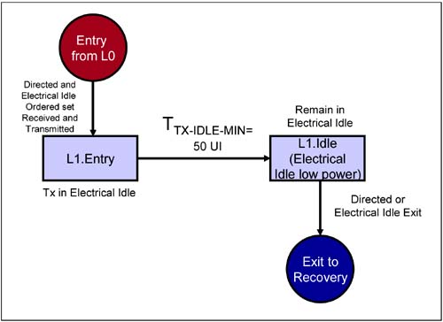
L1.Entry SubState
Entry from L0—
The L0s state machine is entered when a device's higher layer directs the device to do so.
During L1.Entry—
Exit to L1.Idle—
Exit to L1.Idle after 50 UI (20ns), while the transmitter drives a stable DC common mode voltage.
L1.Idle SubState
Entry from L1.Entry—
Enter L1.Idle after 50 UI (20ns), while the transmitter drives a stable DC common mode voltage.
During L1.Idle—
The Link is in the Electrical Idle state. The transmitter's output impedance could be low or high, while the receiver's remains in the low impedance state. Remain in this state until the receiver detects Electrical Idle exit (a valid differential voltage associated with the reception of a TS1 Ordered-Set used to signal L1 exit).
Exit to Recovery—
Exit to Recovery after the receiver detects the Electrical Idle exit condition, or if the device is directed to do so.
L2 State
This is even lower power state than L1 and has a longer exit latency than L1 exit latency. Power Management software directs a device to place its upstream Link into L2 (both directions of the Link go to L2) when the device is placed in a lower power device state such as D3Cold.
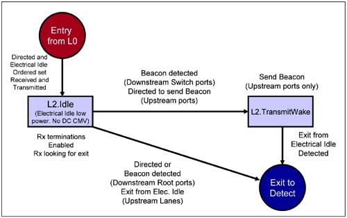
Figure 14-17 on page 544 shows the L2 entry and Exit state machine. This state machine is described next.
L2.Idle SubState
Entry from L0—
This state is entered when directed to do so by higher layers and an Electrical Idle Ordered-Set is exchanged between neighbors across a Link.
During L2.Idle—
The Receiver remains in the low impedance state. The Transmitter must remain in the Electrical Idle state for a minimum of 50 UI (20ns). The Receiver starts looking for the Electrical exit condition. DC common mode voltage doesn't have to be in spec. May be turned off.
Exit to L2.TransmitWake—
When an upstream port is directed to send the Beacon signal due to a wakeup event. Also, when a Beacon is received on at least Lane 0 of a switch downstream port.
Exit to Detect—
When a Beacon is received on at least Lane 0 of a Root Complex downstream port or if a Root Port is directed by a higher layer to go to the Detect state. Also, exit to Detect if an upstream Lane detects the Electrical Idle exit condition.
L1.TransmitWake SubState
Entry from L1.Idle—
Enter into L2.TransmitWake when an upstream port is directed to send the Beacon signal due to a wakeup event. Also, exit to L2.TransmitWake when a Beacon signal is received on at least Lane 0 of a switch downstream port.
During L1.TransmitWake—
Transmit the Beacon signal on at least Lane 0 of the upstream port in the direction of the Root Complex.
Exit to Detect—
Go to Detect if an upstream port detects Electrical Idle exit condition.
Hot Reset State
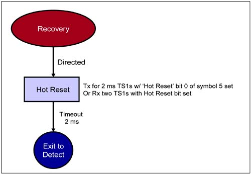
Hot Reset is an in-band signaled reset triggered by software as explained in "In-Band Reset or Hot Reset" on page 491. The state machine in Figure 14-18 on page 545 describes entry to and exit from the Hot Reset state.
Entry from Recovery—
Links that are directed to do so by higher layers enter Hot Reset through the Recovery state.
During Hot Reset—
On all Lanes, the transmitter (on a downstream port) continuously transmits TS1s with the Hot Reset bit set and containing the configured Link and Lane Numbers. The Hot Reset initiator also resets itself. A receiver detects Hot Reset when it detects at least two TS1s with the Hot Reset bit set. It enters the Hot Reset state through recovery. LinkUp = 0.
Exit to Detect—
Exit to detect after a 2ms timeout.
Disable State
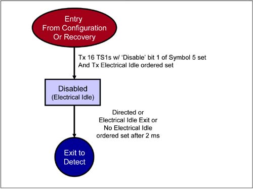
A Disabled Link is a Link that is off and does not have to have the DC common mode voltage driven. If, for example, software wishes to turn off a faulty Link, it can do so by setting the Link Disable bit (see Figure 14-23 on page 553) in the Link Control register of a device. That device transmits TS1s with the Link Disable bit asserted. The state machine in Figure 14-19 on page 546 describes entry to and exit from the Disable state.
Entry from Configuration or Recovery—
All Lanes transmit 16 TS1 Ordered-Sets with the Link Disable bit asserted and then transition to Electrical Idle after transmitting the Electrical Idle Ordered-Set. If no Electrical Idle Ordered-Set is transmitted, then the receiver transitions to the Detect state after 2ms. The DC common mode voltage does not have to be within spec while in Detect.
During Disable—
Exit to Detect—
Exit to detect after a 2ms timeout wherein no Electrical Idle Ordered-set is received, or Disable entry, or an Electrical Idle exit is sensed, or as directed by higher layers.
Loopback State
The Loopback feature is a test and debug feature and is not used in normal operation. A Loopback master device (such as a tester) when connected to a device's Link (the device under test is the Loopback slave when in the Loopback state) can place the Link and Loopback slave into the Loopback state by transmitting TS1 Ordered-Sets with the Loopback bit asserted. The Loopback master can serve as the BIST (Built In Self Test) engine.
Once in this state, the Loopback master sends valid 8b/10b encoded symbols to the Loopback slave. The Loopback slave turns around and feeds back the symbol stream. The Loopback slave continues to perform clock tolerance compensation, so the master must ensure that it inserts Skip Ordered-Sets at the correct intervals. To perform clock tolerance compensation, the Loopback slave may have to add or delete SKP symbols to the Skip Ordered-Set that it feeds back with the symbol stream to the Loopback master. If SKP symbols are added by the Loopback slave, they have to be of the same disparity as the received SKP symbols.
The Loopback state is exited when the Loopback master transmits the Electrical Idle Ordered-Set and the receiver detects that the Link has transitioned to the Electrical Idle state.
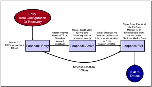
See Figure 14-20 on page 549 for a description of Loopback entry and exit procedure.
Loopback.Entry SubState
Entry—
As directed by higher layers, a Loopback master can transmit TS1 Ordered-Sets with the Loopback bit set.
During Loopback.Entry—
Exit to Loopback.Active—
When the master receives TS1 Ordered-Sets, the slave has entered the Loopback.Active substate.
Exit to Loopback.Exit—
If the master does not receive identical TS1 Ordered-Sets, or does not receive TS1 Ordered-Sets for 100ms, it transitions to the Loopback.Exit state.
Loopback.Active SubState
Entry from Loopback.Entry—
If the master receives TS1s identical to those it transmitted, the slave has entered the Loopback.Active substate.
During Loopback.Active—
The Loopback master transmits valid 8b/10b symbols with valid disparity. The Loopback Slave returns the identical 8b/10b symbos with valid disparity while performing periodically performing clock tolerance compensation.
Exit to Loopback.Exit—
The Loopback master transmits at least 1ms of Electrical Idle Ordered-Sets. A receiver detects Loopback exit when it receives the Electrical Idle Ordered-Set, or senses the Electrical Idle state of the Link.
Loopback.Exit SubState
Entry from Loopback.Active—
The Loopback master transmits at least 1ms of Electrical Idle Ordered-Sets and then enters the Electrical Idle state. A receiver detects Loopback exit when it receives the Electrical Idle Ordered-Set, or senses the Electrical Idle state of the Link.
During Loopback.Exit—
The Loopback master transmits Electrical Idle Ordered-Sets for at least 2ms. The Loopback Slave must enter Electrical Idle on all Lanes for 2ms. Before entering Loopback.Exit, the slave must echo back all symbols it received from the master.
The device then exits to the Detect state.
| 
