| [ Team LiB ] |


|
Link Active State Power ManagementPCI Express includes a feature that requires link power conservation even though the device has not been placed in a low-power state by software. Consequently this feature is call "Active State" power management and functions only when the device is in the DO state. Transitions into and out of Active State Power Management (ASPM) are handled solely by Hardware. Two low power states are defined for ASPM:
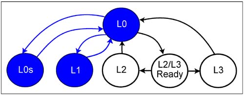
Figure 16-11 illustrates the link state transitions and highlights the transitions between L0, L0s, and L1. Note that transitions between L0s and L1 require the link to be returned to the L0 state. Figure 16-11. ASPM Link State Transitions
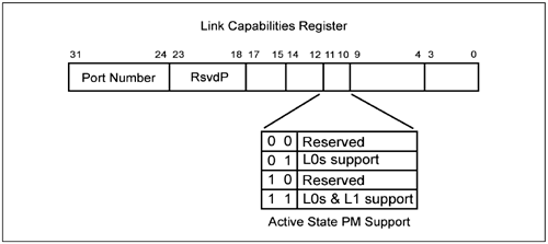
The Link Capability register specifies a device's support for Active State Power Management. Figure 16-12 on page 610 illustrates the ASPM Support field within this register. Notice that the only two combinations are supported via this register:
Figure 16-12. ASPM Support
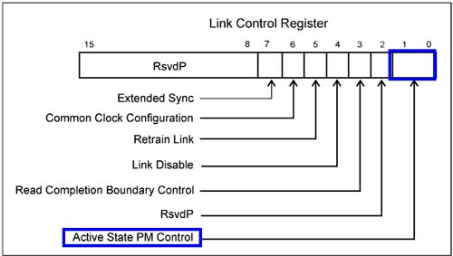
Software can enable and disable ASPM via the Active State PM Control field of the Link Control Register as illustrated in Figure 16-13 on page 611. The possible settings are listed in Table 16-18 on page 610. The following discussion of ASPM presume that the related features are enabled. Figure 16-13. Active State PM Control Field
Note: The specification recommends that ASPM be disabled for all components in the path associated with Isochronous transactions, if the additional latencies associated with ASPM exceeds the limits of the isochronous transactions.
L0s StateL0s is a link power state that can be entered by any port and applied to a single direction of the link. For example, a large volume of traffic in conventional PC-based systems results from PCI and PCI Express devices sending data to main system memory. This means that the upstream lanes will have heavy traffic, while the downstream lanes will carry occasional ACK TLPs. These downstream lanes can enter the L0s state to conserve power during the stretches of idle bus time. Entry into L0sA transmitting port initiates the transition from L0 to L0s after detecting a period of idle time on the transmit link. Details regarding the meaning of idle, how L0s is entered, and the resulting transmitter and receiver states after L0s has been entered is discussed in this section. Entry into L0s Triggered by Link Idle TimeEntry into L0s is managed for a single direction of the link based on detecting a period of link idle time. Ports are required to enter L0s after detecting idle time of no greater than 7µs. Idle is defined by the specification differently for each category of device. Each category must satisfy the bulleted items listed to be considered in the idle state:
The Transaction and Data Link Layers have no knowledge of whether the transmitting side of the Physical Layer has entered L0s; however, the conditions that trigger a transition to L0s must be continuously reported from the Transaction and Link layers to the Physical Layer. Note that the receiving side of a port must always support entering L0s even if software has disabled ASPM for this port. This allows a device at the other end of the link (that is enabled for ASPM) to still transition one side of the link to the L0s state. Flow Control Credits Must be DeliveredA pending TLP that cannot be sent due to insufficient FC credits satisfies one of the requirements for an idle condition for all device categories listed above. Consequently, if flow control credits are received during L0s that permits delivery of the pending TLP, the transmitting port must initiate the return to L0. Also, if the receive buffer (associated with the transmit side that is in L0s) makes additional flow control credits available, a transmitter must initiate the return to L0 and deliver the related FC_Update DLLP to the port at the opposite end of the link. Transmitter Initiates Entry to L0sWhen sufficient idle time has been observed on the transmit side of the link, the transmitter forces the transition from L0 to L0s by taking the following steps. Following the sequence of events, both the transmitter and receiver will have transitioned to L0s:
The transmitter and receiver are now in their electrical idle states and have reduced power consumption. Synchronization between the transmitter and receiver has been lost and retraining is required. The specification requires that the PLL in the receiver must remain active to allow quick re-synchronization and recovery from L0s back to L0. Exit from L0s StateIf the transmitter detects that the idle condition has disappeared, it must initiate the sequence necessary to exit L0s and a return to L0. The specification encourages designers to monitor events that give an early indication that L0s exit is imminent and to start the recovery process to speed up the transition back to L0. For example, if the receiving side of the link receives a non-posted TLP, the transmitter side knows that it will shortly receive a request to send a completion transaction. Consequently, the transmitter can start the transition back to L0 prior to receiving the completion request. Transmitter Initiates L0s ExitWhen the transmitter whether in the upstream or downstream component recognizes that it must transition the link from L0s to L0, it initiates a sequence that re-establishes the connection with the receiver:
Actions Taken by Switches that Receive L0s ExitA switch's receiving port in the L0s state that receives the L0s to L0 transition sequence must also transmit an L0s exit to other switch ports currently in the L0s state. Two specific cases must be considered:
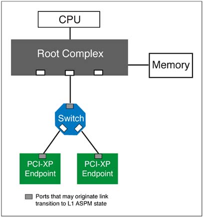
Any switch port in the L1 state (not L1 ASPM) has been placed into L1 due to software having previously transitioned the device to a D1 or higher power savings state. These ports remains unaffected by L0s to L0 transitions. However, once the upstream link has completed the transition to L0, a subsequent transaction may target this port, causing a transition from L1 to L0. L1 ASPM StateThe optional L1 ASPM state provides power savings greater than L0s, but with the cost of much greater recovery latency. This state also results in both directions of the link being placed into the L1 state and results in Link and Transaction layer deactivation within each device. Entry into this state is initiated only by the downstream component (an endpoint or the upstream port of a switch). Note that a switch may support L1 ASPM on any combination of its ports. The port at the opposite end of the link can be a root port or the downstream port of a switch. In either case, the upstream component must agree to enter the L1 state through a negotiation process with the downstream component. (See Figure 16-14 on page 615) Note that exiting the L1 ASPM state can be initiated by either the downstream or upstream port. Figure 16-14. Ports that Initiate L1 ASPM Transitions
Downstream Component Decides to Enter L1 ASPMThe specification does not precisely define all conditions under which an endpoint or upstream port of a switch decides to attempt entry into the L1 ASPM state. The specification does suggest that one requirement might be that both directions of the link have entered L0s and have been in this state for a preset amount of time. The requirements specified include:
Negotiation Required to Enter L1 ASPMBecause of the long latency required to recover from L1 ASPM, a negotiation process is employed to ensure that the port at the other end of the link is enabled for L1 ASPM entry and is prepared to enter it. The negotiation involves sending several transactions:
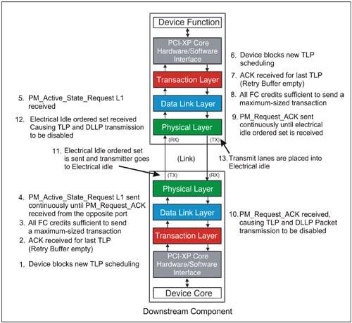
The upstream component may or may not accept the transition to the L1 ASPM state. The following scenarios describe a variety of circumstances that result in both conditions. Scenario 1: Both Ports Ready to Enter L1 ASPM StateFigure 16-15 on page 618 summarizes the sequence of events that must occur to enable transition to the L1 ASPM state. This scenario assumes that all transactions have completed in both directions and no new transaction requirements emerge during the negotiation. Figure 16-15. Negotiation Sequence Required to Enter L1 Active State PM
Downstream Component Issues Request to Enter L1 StateOnce the downstream component has fulfilled all the requirements to transition to the L1 state, it can issue the request to enter L1 once the following steps have completed:
The downstream component delivers the PM_ Active_State_Request_L1 DLLP to notify the upstream component of the request to enter the L1 state. This transaction is sent repeatedly until the upstream component returns a response — either a PM_Request_ACK DLLP or a PM_Active_State_NAK TLP. Upstream Component Requirements to Enter L1 ASPMAs illustrated in Figure 16-14 on page 615 the upstream component may be either a Root Complex Port, or a Switch Downstream Port. These ports must accept a request to enter a low power L1 state if all of the following conditions are true:
Upstream Component Acknowledges Request to Enter L1The upstream component sends a PM_Request_ACK DLLP to notify the downstream component of its agreement to enter the L1 ASPM state. Prior to sending this acknowledgement, it must complete the following:
The Upstream component then sends a PM_Request_Ack DLLP and continues sending the transaction continuously until it receives the Electrical Idle ordered set on its receive lanes. Downstream Component Detects AcknowledgementWhen the Downstream component detects a PM_Request_Ack DLLP, it knows that the upstream device has accepted the request. In response, the downstream component stops sending the PM_Active_State_Request_L1 DLLP, disables DLLP and TLP transmission, and places its transmit (upstream) lanes into the Electrical Idle state. Upstream Component Receives Electrical IdleWhen the Upstream component receives an Electrical Idle ordered set on its Receive Lanes (signaling that the Downstream component has entered the L1 state), it then stops sending the PM_Request_Ack DLLP, disables DLLP and TLP transmission, and places its transmit (downstream) lanes into the Electrical Idle state. Scenario 2: Upstream Component Transmits TLP Just Prior to Receiving L1 RequestThis scenario presumes that the upstream component has just received a request to send a TLP to the downstream component as it prepares to request entry in to the L1 state. Currently, the downstream device is unaware of the TLP being sent and the upstream device is unaware of the request to entry L1. Several negotiation rules define the actions that ensure that this situation is managed correctly. TLP Must Be Accepted by Downstream ComponentNote that after the downstream device sends the PM_Active_State_L1 DLLP it must wait for a response from the upstream component. While waiting, the receive side of the downstream component must be able to accept TLPs and DLLPs from the upstream device. Furthermore, it must also be able to send a DLLP as required. In this example the downstream component must respond to the TLP. Two possibilities exist:
In summary, the specification requires that all TLPs be acknowledged prior to entering the L1 state. Upstream Component Receives Request to Enter L1The specification requires that the upstream component immediately accept or reject the request to enter the L1 state. However, it further states that prior to sending a PM_Request_ACK DLLP it must:
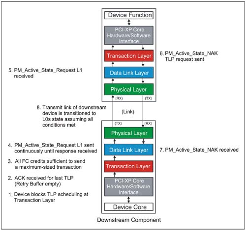
Once all outstanding TLPs have been acknowledged, and all other conditions are satisfied, the upstream device must return a PM_Request_ACK DLLP. Scenario 3: Downstream Component Receives TLP During NegotiationDuring the negotiation sequence the downstream device may receive a new TLP targeting the upstream device. Recall that when a device begins the L1 ASPM negotiation process, it must block new TLP scheduling. This prevents a race condition between completing the transition to L1 and sending a new TLP that would otherwise prevent entry into L1 ASPM. Consequently, once all requirements to enter L1 have been satisfied and the downstream device has scheduled delivery of the PM_Request_L1 DLLP it must complete the transition to the L1 state (if a PM_Request_ACK is received). Then it can initiate the transition from L1 ASPM to L0 and send the TLP. Scenario 4: Upstream Component Receives TLP During NegotiationNote that in the event that the upstream component needs to transfer a TLP or DLLP after sending the PM_Request_Ack DLLP, it is required to complete the transition to L1. It must then initiate a transition from L1 to L0, after which the TLP or DLLP can be sent. Scenario 5: Upstream Component Rejects L1 RequestFigure 16-16 on page 621 summarizes the negotiation sequence when the upstream component rejects the request to enter the L1 ASPM state. Figure 16-16. Negotiation Sequence Resulting in Rejection to Enter L1 ASPM State
The negotiation begins normally with the downstream component sending the request DLLP to enter L1. However, the upstream device returns a PM_Active_State_Nak TLP to indicate rejection of the request. The reasons for the upstream component rejecting the request to enter L1 include:
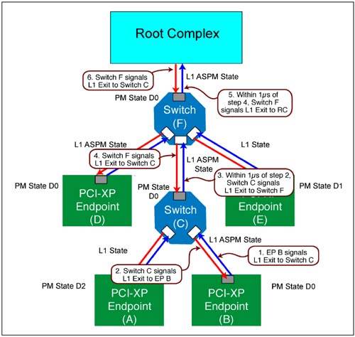
Once the upstream component sends the rejection message, it can send TLPs and DLLPs as required. If the downstream component receives a rejection it must transition to L0s if possible. Exit from L1 ASPM StateEither component can initiate the transition from L1 to L0 when it needs to communicate via the link. Whether the upstream or downstream component initiates the exit from L1, the procedure is the same and does not involve any negotiation as does L1 entry. When switches are involved in exiting from L1 the specification requires that other switch ports in the ASPM low power states must also transition to the L0 state if they are possibly in the path of the transaction causing the exit. These issues are discussed in subsequent sections. L1 ASPM Exit SignalingThe specification states that exit from L1 is invoked by exiting electrical idle, which could consist of a variety of signaled states. However, because re-training (recovery) is required to transition the link back to the L0 state, it seems reasonable that exit signaling would begin by transmitting the TS1 ordered set to the opposite port. The receiving port, in turn initiates recovery by signaling the TS1 ordered set back to the originating devices's receive port. The Physical Layer's Link Training State Machine completes the Recovery state after which the link will be returned to L0. Refer to"Recovery State" on page 532 for details. Switch Receives L1 Exit from Downstream ComponentThis sections describes the switch behavior when a downstream component initiates exit from L1 (TS1 ordered set) to the switch. As pictured in Figure 16-17 on page 623, the Switch must respond to L1 exit signaling by returning the TS1 ordered set to the downstream component, and within 1µs (from signal L1 Exit downstream) it must also transmit the TS1 ordered set on its upstream link (but only when the upstream port is also in the L1 ASPM state). Figure 16-17. Switch Behavior When Downstream Component Signals L1 Exit
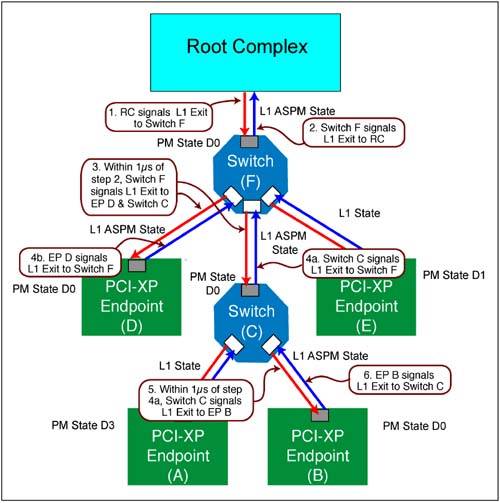
The expectation is that the downstream component, having initiated L 1 exit, is preparing to send a TLP traveling in the upstream direction. Because L1 exit latencies are relatively long, the specification states that a switch "must not wait until its Downstream Port Link has fully exited to L0 before initiating an L1 exit transition on its Upstream Port Link." This prevents accumulated latencies that would otherwise result if all L1 to L0 transitions occurred in a linear fashion. Switch Receives L1 Exit from Upstream ComponentThis section describes the switch behavior when an upstream component signals L1 Exit (TS1 ordered set) to a switch. In this case, the switch must send the TS1 ordered set back upstream, and within 1µs it must also signal the TS1 ordered set to force all downstream ports that are in the L1 ASPM state to also return to L0. The goal as in the previous example is to shorten the overall latency in returning to the L0 state. Figure 16-18 on page 624 summarizes these requirements. Note that the link attaching Switch F and EndPoint (EP) E is in the L1 state due to software having previously placed EP E into the D1 state, which caused the link to transition to L1. Only links in the L1 ASPM state are transitioned to L0 as a result of the Root Complex (RC) initiating the exit from L1 ASPM. Figure 16-18. Switch Behavior When Upstream Component Signals L1 Exit
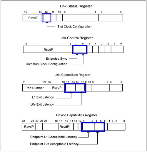
ASPM Exit LatencyPCI Express provides the mechanisms to ensure that the ASPM exit latencies for L0s and L1 do not exceed the latency requirements of the endpoint devices. Each device must report its L0s and L1 exit latencies from the moment ASPM exit is signaled. Endpoints also report the total acceptable latency that they can tolerate when performing accesses (typically to and from main memory). This latency is a function of the data buffer size within the device. If the chain of devices that reside between the endpoint and target device have a total latency that exceeds the acceptable latency reported by the endpoint, software can disable ASPM to avoid unacceptable latency for a given endpoint. The exit latencies reported by a device will change depending on whether the devices on each end of a link share a common reference clock or not. Consequently, the Link Status register includes a bit called Slot Clock that specifies whether the component uses an external reference clock provided by the platform, or an independent reference clock (perhaps generated internally). Software checks these bits within devices at both ends of each link to determine whether they use a common clock. If so, software sets the Common Clock bit to report the common clock implementation to both devices. Figure 16-20 on page 628 illustrates the registers and related bit fields involved in managing the ASPM exit latency. Figure 16-20. Config. Registers Used for ASPM Exit Latency Management and Reporting
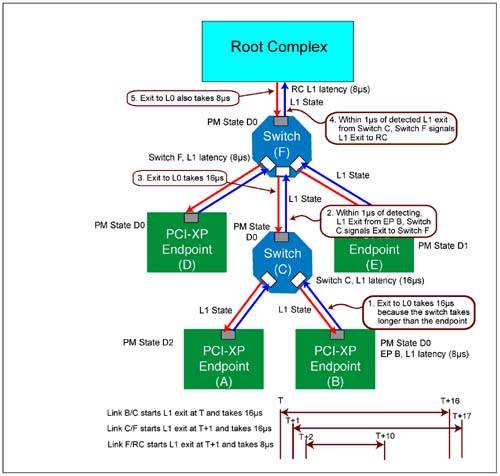
Reporting a Valid ASPM Exit LatencyBecause the clock configuration affects the exit latency that a device will experience, devices must report the source of their reference clock via the Slot Clock status bit within the Link Status register. This bit is initialized by the component to report the source of its reference clock. If this bit is set (1), the clock uses the platform generated reference clock and cleared (0) if it uses an independent clock. If system firmware or software determines that the components at each end of the link use the platform clock then the reference clocks within both devices will be in phase. This results in shorter exit latencies from L0s and L1, and is reported in the Common Clock field of the Link Control register. Components must then update their reported exit latencies to reflect the correct value. Note that if the clocks are not common then the default values will be correct and no further action is required. L0s Exit Latency UpdateExit latency for L0s is reported in the Link Capability register based on the default assumption that a common clock implementation does not exist. L0s exit latency is also reported during link training (via the TS1 Ordered Sets) by specifying the number of FTS Ordered Sets (N_FTS) required to exit L0s. Consequently, if software detects a common clock implementation, the Common Clock field is set and System firmware or software must write to the Retrain Link bit in the Link Control register, to force retraining. During retraining new N_FTS values are reported to the transmitter at the opposite end of the link and new values are also reported in L0s Latency field of the Link Capability register. L1 Exit Latency UpdateFollowing link retraining, new values will also be reported in the L1 Latency field. Calculating Latency Between Endpoint to Root ComplexFigure 16-19 on page 627 illustrates an endpoint whose transactions must transverse 2 switches in the path between the endpoints and Root Complex. This example presumes that all links in the path are in the L1 state.
Figure 16-19. Example of Total L1 Latency
 |
| [ Team LiB ] |
|