| [ Team LiB ] |


|
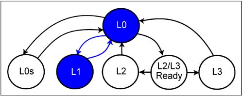
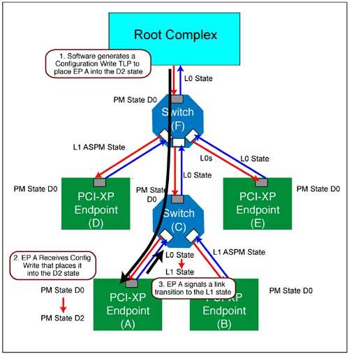
Software Initiated Link Power ManagementWhen software initiates configuration write transactions to transition the power state of a device to conserve power, devices must respond by transitioning their link to the corresponding low power state. D1/D2/D3Hot and the L1 StateThe specification requires that when all functions within a device have been placed into any of the low power states (D1, D2, or D3hot) by software, the device must initiate a transition to the L1 state. A device returns to L0 as a result of software intitiating a configuration access to the device or due to a device initiated Power Management Event (PME). See Figure 16-21. Figure 16-21. Devices Transition to L1 When Software Changes their Power Level from D0
Upon receiving a configuration write transaction to the Power State field of the PMCSR register a device initiates the transition from L0 to L1 by sending a PM_Enter_L1 DLLP to the upstream component. Figure 16-22 on page 630 illustrates the sequence of events. In the example, software places the EndPoint (EP) device into the D2 state. Figure 16-22. Software Placing a Device into a D2 State and Subsequent Transition to L1
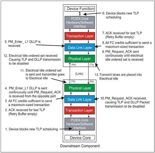
Entering the L1 StateThe procedure required to place the link into an L1 state is illustrated in Figure 16-23 on page 632. Each step referenced in the figure is described in greater detail below:
Figure 16-23. Procedure Used to Transition a Link from the L0 to L1 State
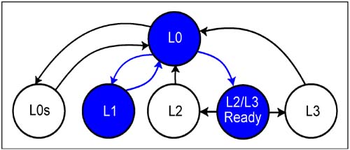
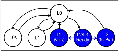
Exiting the L1 StateThe exit from the L1 state can be initiated by either the upstream or downstream component. The trigger that causes an exit from L1 back to L0 is different for upstream and downstream devices as discussed below. This section also summarizes the signaling protocol used to exit L1. Upstream Component Initiates L1 to L0 TransitionSoftware having placed a device into a power saving state (D1, D2, or D3) may need to transition the device back to D0 to permit device access. Power Management software must issue a configuration write transaction to change the power state back to D0. When the configuration transaction arrives at the upstream component (a Root Port or downstream Switch Port) the port will exit the electrical idle state which initiates re-training and return of the link to the L0 state. Once the link is active, the configuration write transaction can be delivered to the device causing the transition back to D0. The device is now ready for normal operation again. Downstream Component Initiates L1 to L0 TransitionWhen a link is in the L1 state the reference clock is still active and power is still applied to devices attached to the link. A downstream device may be designed to monitor external events that would trigger a Power Management Event (PME). In conventional PCI, a PME is reported via a signal of the same name — PME#. This signal is routed to system board logic that is responsible for notifying software (typically via an interrupt) of the need to exit L1. PCI Express uses the same concept but eliminates the sideband signal with a virtual wire message that reports the PME. (See "The PME Message" on page 639 for details.) The L1 Exit ProtocolWhen in the L1 state both directions of the link are in the electrical idle state. A device signals an exit from L1 by transmitting the TS1 Ordered Sets, thereby causing the exit from electrical idle. When the device at the other end of the link detects the exit from electrical idle it sends the TS1 Ordered Sets back to the originating device. This sequence triggers both devices to enter re-training (recovery). Following recovery both devices will have returned to the L0 state. L2/L3 Ready — Removing Power from the LinkOnce software has placed all functions within a device into the D3hot state power can be removed from the device. A typical application for this would be to place all devices in the fabric into D3 and put all devices to sleep by removing power to all devices. Depending on the system design power can also be removed from devices selectively based on the implementation of separate power planes that permits power to be removed selectively. The specification does not specify the actual mechanism that would be used to remove clock and power (main power rails). The state transitions required to prepare devices for removing power involve the preliminary steps of entering L1 and then via a handshake protocol returning to L0 and then to the L2/L3 Ready state as illustrated in Figure 16-24. Figure 16-24. Link States Transitions Associated with Preparing Devices for Removal of the Reference Clock and Power
L2/L3 Ready Handshake SequenceThe specification however requires a handshake sequence when transitioning to the L2/L3 Ready state. This handshake has two purposes:
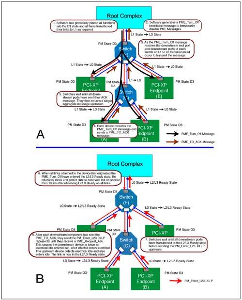
Below is an example of the handshake sequence that is required before removing the reference clock and power from all PCI Express devices in the fabric. This example assumes a system-wide power down is being initiated. However the sequence can also apply to smaller segments of the PCI Express fabric or individual devices. The required steps are summarized below and in Figure 16-25 on page 636 (which illustrates a single Root Port). The overall sequence is represented in two parts labeled A and B. The Link transitions involved in the complete sequence include:
Figure 16-25. Negotiation for Entering L2/L3 Ready State
The following steps detail the sequence illustrated in Figure 16-25.
Exiting the L2/L3 Ready State — Clock and Power RemovedAs illustrated in the state diagram in Figure 16-26, a device may only exit the L2/L3 Ready state when power is removed. Note that when Vaux is available the transition is to L2 and when all power is removed the transition is to L3. Figure 16-26. State Transitions from L2/L3 Ready When Power is Removed
Link state transitions are normally under control of the Link Training Sequence State Machine (LTSSM) within the Physical Layer. However, transitions to the L2 and L3 states result from main power being removed. Because the LTSSM operates typically on main power only, the specification refers to the L2 and L3 states as pseudo-states. These states are defined for explaining the resulting condition of a device when power is removed under Power Management software control, and are not associated with LTSSM actions. The L2 StateSome devices are designed to monitor external events and initiate a wakeup sequence so that an external event can be handled normally. Because main power is removed from the device, these device may need AUX power to monitor the events and to signal wakeup to notify software that the device needs to be revived. The L3 StateWhen in this state the device has no power and therefore no means of communication. Recovery from this state requires the system to re-establish power and reference clock and receive fundamental reset.  |
| [ Team LiB ] |
|