| [ Team LiB ] |


|
Link Wake Protocol and PME GenerationThe wake protocol provides a method for devices to reactivate the upstream link and request that Power Management software return the devices to D0 so they can perform required operations. The procedures and signaling methods used in PCI Express are different from the PCI-PM specified methods. However, PCI Express PM is designed to be compatible with PCI-PM software. Rather than using the PCI-defined PME# sideband signal, PCI Express devices employ an inband PME message to notify PM software of a request to return the device to the full power state (D0). The ability to generate PME messages may be supported optionally within any of the low power states. Recall that devices report the PM states they support and from which of these states they can send a PME message. See Figure 16-8 on page 597. PME messages can only be delivered once the link power state transitions to L0. The level of difficulty and latency required to reactivate the link so that a PME message can be sent is a function of a device's PM and Link state. Consequently, the steps required to complete a wakeup can include the following depending on the current link state:
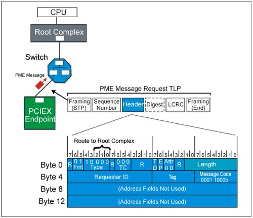
The PME MessageThe PME message is delivered by devices that support PME notification. The message format is illustrated in Table 16-27 on page 639. The message may be initiated by a device in a low power state (D1, D2, D3hot, and D3cold) and is sent immediately upon return of the link to L0. Figure 16-27. PME Message Format
The PME message is a Transaction Layer Packet that has the following characteristics:
The PME SequenceDevices may support PME in any of the low power states as specified in the PM Capabilities register. This register also specifies the amount of AUX current required by the device if it supports wakeup in the D3cold state. The basic sequence of events associated with signaling a PME to software is specified below and presumes that the device and system are enabled to generate PME (See "Scenario—Setup a Function-Specific System WakeUp Event" on page 583.) and the link has already been transitioned to the L0 state:
PME Message Back Pressure Deadlock AvoidanceThe specification describes a potential deadlock scenario that is solved by specifying a PCI Express rule. The problem and solution are described below: BackgroundThe Root Complex typically stores the PME messages it receives in a queue, and calls PM software to handle each PME. A PME is held in this queue until PM software reads the PME_Status bit from the requesting device's PMCSR register. Once the configuration read transaction completes, this PME message can be removed from the internal queue. The ProblemDeadlock can occur if the following scenario develops:
The SolutionThe deadlock is avoided if the Root Complex accepts any arriving PME messages, even when these message would overflow the queue. However, the Root Complex in this case simply discards the incoming PME message, because there is no place to store it. Consequently, the PME message is lost. Note that acceptance of a PME message still requires sufficient flow control credits. To prevent a discarded PME message from being lost permanently, the device that sends a PME message is required to re-send it following a time-out interval, called the PME Service Time-out. If after sending a PME message, the device's PME_Status bit is not cleared with 100 ms (+ 50%/- 5%), it must re-issue the message. The PME ContextDevices that generate PME must continue to power portions of the device that are used for detecting, signaling, and handling PME events. These items are called the PME context. Devices that support PME in the D3cold state use AUX power to maintain the PME context when the main power is removed. Following is a list of items that are typically part of the PME context.
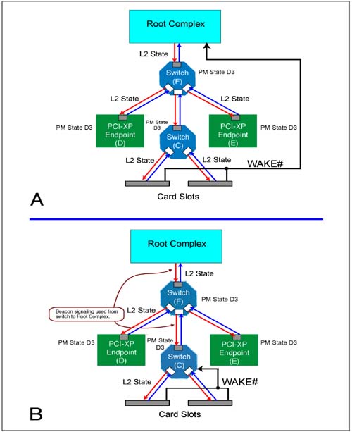
Waking Non-Communicating LinksWhen a device that supports PME in the D3cold state needs to send a PME message, it must first initiate the sequence of events needed to transition the link to the L0 state so that the message can be sent. This is typically referred to as wakeup. PCI Express defines two methods of triggering the wakeup of non-communicating links: In both cases, PM software must be notified so that it can re-apply main power and restart the reference clock. This also causes generation of fundamental reset that forces a device into the D0uninitialized state. Once the link transitions to the L0 state, the device sends the PME message. Because reset is required to re-activate the link so that PME can be signaled, devices must maintain PME context across the reset sequence described above. BeaconPCI Express includes a signaling mechanism designed to operate on AUX power that does not require the differential drivers and receivers to be used. The beacon is simply a way of notifying the upstream component that software should be notified of the wakeup request. Switches upon receiving beacon on one of their downstream ports signal beacon on the upstream port. Ultimately, the beacon signal reaches the root complex, causing an interrupt that calls PM software. Some form-factor types require support for the beacon signalling for waking the system, while others do not. The specification requires compliance with the specific form-factor specifications, and does not require beacon support for devices used in form-factors not requiring this support. However, for "universal" PCI Express components (those designed for use in a variety of form-factors) beacon support is required. See "Beacon Signaling" on page 469 for details. WAKE# (AUX Power)PCI Express also provides a sideband signal called WAKE#, as a alternative to beacon signaling. This signal may be routed directly to the Root Complex or other motherboard logic, thereby causing an interrupt that will call PM software. It's also possible that a hybrid implementation can be used. In this case, WAKE# is sent to a switch, which in turn signal beacon on its upstream port. The options are illustrated in Figure 16-28 on page 644 A and B. Note that when asserted, the WAKE# signal remains low until the PME_Status bit is cleared by software. Figure 16-28. WAKE# Signal Implementations
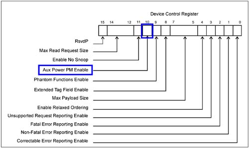
This signal must be implemented by ATX or ATX-based form factor and by the minis. motherboard connectors and cards as well as for the mini-card form factor. No requirement is specified for embedded devices to use the WAKE# signal. Auxiliary PowerDevices that support PME in the D3cold state must support the wakeup sequence (via beacon signaling or the sideband Wake# pin) and are allowed to consume the maximum auxiliary current of 375 mA (20mA maximum otherwise). The amount of current that they need is reported via the Aux_Current field within the PM Capability registers. Auxiliary power is enabled when the PME_Enable bit is set within the PMCSR register. PCI-PM limits the use of Auxiliary Current as specified above. PCI Express extends the use of auxiliary power beyond the limitations specified by PCI-PM. Now devices that have PME disabled or that do not support PME can also consume the maximum amount of auxiliary current allowed. This new capability is enabled via software by setting the Aux Power PM Enable bit in the Device Control register, illustrated in Figure 16-29 on page 645. This capability permits devices the opportunity to support other functions such as SM Bus functionality while in a low power state. As in PCI-PM the amount of current consumed by a device is reported in the Aux_Current field in the PMC register. Figure 16-29. Auxiliary Current Enable for Devices Not Supporting PMEs
|
| [ Team LiB ] |
|