PCI-Compatible Configuration Mechanism
For x86-based PC-AT compatible systems, the 2.3 PCI spec defines a method that utilizes processor-initiated IO accesses to instruct the host/PCI bridge (in this case, within the Root Complex) to perform PCI configuration accesses.The spec does not define a configuration mechanism to be used in systems other than PC-AT compatible systems.
Background
The x86 processor family is capable of addressing up to, but no more than, 64KB of IO address space. In the EISA spec, the usage of this IO space was defined in such a manner that the only IO address ranges available for the implementation of the PCI Configuration Mechanism (without conflicting with an ISA or EISA device) were 0400h - 04FFh, 0800h - 08FFh, and 0C00h - 0CFFh. Many EISA system board controllers already resided within the 0400h - 04FFh address range, making it unavailable.
Consider the following:
As with any other PCI function, a host/PCI bridge may implement up to 64 dwords of configuration registers. Each PCI function on each PCI bus requires 64 dwords of dedicated configuration space.
Due to the lack of available IO real estate within the 64KB of IO space, it wasn't feasible to map each configuration register directly into the processor's IO address space. Alternatively, the system designer could implement the configuration registers within the processor's memory space. The amount of memory space consumed aside, the address range utilized would be unavailable for allocation to regular memory. This would limit the system's flexibility regarding the mapping of actual memory.
PCI-Compatible Configuration Mechanism Description
General
The PCI-Compatible Configuration Mechanism utilizes two 32-bit IO ports implemented in the Host/PCI bridge within the Root Complex, located at IO addresses 0CF8h and 0CFCh. These two ports are:
The 32-bit Configuration Address Port, occupying IO addresses 0CF8h through 0CFBh. The 32-bit Configuration Data Port, occupying IO addresses 0CFCh through 0CFFh.
Accessing one of a function's PCI-compatible configuration registers is a two step process:
Write the target bus number, device number, function number and dword number to the Configuration Address Port and set the Enable bit in it to one. Perform a one-byte, two-byte, or four-byte IO read from or a write to the Configuration Data Port.
In response, the host/PCI bridge within the Root Complex compares the specified target bus to the range of buses that exist on the other side of the bridge and, if the target bus resides beyond the bridge, it initiates a configuration read or write transaction (based on whether the processor is performing an IO read or write with the Configuration Data Port).
Configuration Address Port
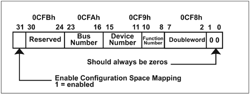
Refer to Figure 20-2 on page 726. The Configuration Address Port only latches information when the processor performs a full 32-bit write to the port. A 32-bit read from the port returns its contents. The assertion of reset clears the port to all zeros. Any 8- or 16-bit access within this IO dword is treated as an 8- or 16-bit IO access. The 32-bits of information written to the Configuration Address Port must conform to the following template (illustrated in Figure 20-2 on page 726):
bits [1:0] are hard-wired, read-only and must return zeros when read. bits [7:2] identify the target dword (1-of-64) within the target function's PCI-compatible configuration space. When the Root Complex subsequently generates the resultant configuration request packet, this bit field supplies the content of the packet's Register Number field and the packet's Extended Register Number field is set to all zeros. This configuration access mechanism is therefore limited to addressing the first 64 dwords of the targeted function's configuration space (i.e., the function's PCI-compatible address space). bits [10:8] identify the target function number (1-of-8) within the target device. bits [15:11] identify the target device number (1-of-32). bits [23:16] identifies the target bus number (1-of-256). bits [30:24] are reserved and must be zero. bit 31 must be set to a one, enabling the translation of a subsequent processor IO access to the Configuration Data Port into a configuration access. If bit 31 is zero and the processor initiates an IO read from or IO write to the Configuration Data Port, the transaction is treated as an IO transaction request.
Bus Compare and Data Port Usage
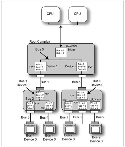
Refer to Figure 20-3 on page 728. The Host/PCI bridge within the Root Complex implements a Bus Number register and a Subordinate Bus Number register. In a chipset that only supports one Root Complex, the bridge may have a bus number register that is hardwired to 0, a read/write register that reset forces to 0, or it just implicitly knows that it is the bridge to bus 0. If bit 31 in the Configuration Address Port (see Figure 20-2 on page 726) is enabled (i.e., set to one), the bridge compares the target bus number to the range of buses that exists beyond the bridge.
Target Bus = 0
If the target bus is the same as the value in the Bus Number register, this is a request to perform a configuration transaction on bus 0. A subsequent IO read from or write to the bridge's Configuration Data Port at 0CFCh causes the bridge to generate a Type 0 configuration read or write transaction. When devices that reside on a PCI bus detect a Type 0 configuration transaction in progress, this informs them that one of them is the target device (rather than a device on one of the subordinate buses beneath the bus the Type 0 transaction is being performed on).
Bus Number < Target Bus  Subordinate Bus Number Subordinate Bus Number
If the target bus specified in the Configuration Address Port is > than the value in the bridge's Bus Number register, but is the value in the bridge's Subordinate Bus Number register, the bridge converts the subsequent processor IO access to its Configuration Data Port into a Type 1 configuration transaction on bus 0. When devices (other than PCI-to-PCI bridges) that reside on a bus detect a Type 1 configuration access in progress, they ignore the transaction.
The only devices on a bus that pay attention to the Type 1 configuration transaction are PCI-to-PCI bridges. Each of them must determine if the target bus number (delivered in the packet's header) is within the range of buses that reside behind them:
If the target bus is not within range, then a PCI-to-PCI bridge ignores the Type 1 access. If it's in range, the access is passed through the PCI-to-PCI bridge as either a Type 0 configuration transaction (if the target bus = the bus number in the bridge's Secondary Bus Number register), or as a Type 1 transaction (if the target bus number the value in the bridge's Subordinate Bus Number register and > than the value in the bridge's Bus Number register).
The subject of Type 0 configuration accesses is covered in detail in "Type 0 Configuration Request" on page 732. The subject of Type 1 configuration accesses is covered in detail in "Type 1 Configuration Request" on page 733.
Single Host/PCI Bridge
Refer to Figure 20-3 on page 728. The information written to the Configuration Address Port is latched by the Host/PCI bridge within the Root Complex. If bit 31 is set to one and the target bus number = the value in the bridge's Bus Number register (or is the value in the bridge's Subordinate Bus Number register), the bridge is enabled to convert a subsequent processor access targeting its Configuration Data Port into a configuration access on bus 0 within the Root Complex. The processor then initiates a one-byte, two-byte, or four-byte (for an x86 processor indicated by the processor's byte enable signals; or, if a PowerPC 60x processor, by A[29:31] and TSIZ[0:2]) IO read or write transaction to the Configuration Data Port at 0CFCh. This stimulates the bridge to perform a configuration read (if the processor is reading from the Configuration Data Port) or a configuration write (if the processor is writing to the Configuration Data Port). It will be a Type 0 configuration transaction if the target bus is bus 0, or a Type 1 configuration transaction if the target bus is further out in the bus hierarchy beyond bus 0.
Multiple Host/PCI Bridges
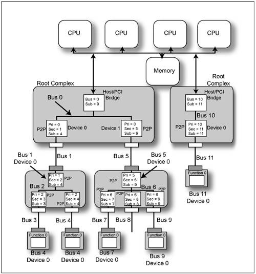
If there are multiple Root Complexes present on the processor's FSB (refer to Figure 20-4 on page 730), the Configuration Address and Data ports are duplicated at the same IO addresses in each of their respective host/PCI bridges. In order to prevent contention on the processor's FSB signals, only one of the bridges responds to the processor's accesses to the configuration ports.
When the processor initiates the IO write to the Configuration Address Port, only one of the host/PCI bridges actively participates in the transaction. The other bridge quietly snarfs the data as it's written to the active participant. Both bridges then compare the target bus number to their respective Bus Number and Subordinate Bus Number registers. If the target bus doesn't reside behind a particular host/PCI bridge, that bridge doesn't convert the subsequent access to its Configuration Data Port into a configuration access on its bus (in other words, it ignores the transaction). A subsequent read or write access to the Configuration Data Port is only accepted by the host/PCI bridge that is the gateway to the target bus. This bridge responds to the processor's transaction and the other ignores it. When the access is made to the Configuration Data Port, the bridge with a bus compare tests the state of the Enable bit in its Configuration Address Port. If the Enabled bit = 1, the bridge converts the processor's IO access into a configuration access: If the target bus is the bus immediately on the other side of the Host/PCI bridge, the bridge converts the access to a Type 0 configuration access on its secondary bus. Otherwise, it converts it into a Type 1 configuration access.
|

