PCI-Compatible Capabilities
AGP Capability
The 2.2 spec assigns the Capability ID of 02h to AGP. The remainder of this section is only included as an example of a New Capability.
Refer to Figure 22-25 on page 845.
The AGP's Capability ID is 02h. The second byte is the register that points to the register set associated with the next New Capability (if there is one). Following the pointer register are two, 4-bit read-only fields designating the major and minor rev of the AGP spec that the AGP device is built to (at the time of this writing, the major rev is 2h and the minor is 0h). The last byte of the first dword is reserved and must return zero when read. The next two dwords contain the AGP device's AGP Status and AGP Command registers.
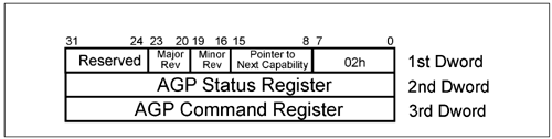
The sections that follow define these registers and the bits within them.
For a detailed description of AGP, refer to the MindShare book entitled AGP System Architecture (published by Addison-Wesley).
AGP Status Register
The AGP Status register is defined in Table 22-10 on page 846. This is a read-only register. Writes have no effect. Reserved or unimplemented fields or bits always return zeros when read.
Table 22-10. AGP Status Register (Offset CAP_PTR + 4)|
31:24 | RQ | The RQ field contains the maximum depth of the AGP request queue. Therefore, this number is the maximum number of transaction requests this device can manage. A "0" is interpreted as a depth of one, while FFh is interpreted as a depth of 256. | 23:10 | Reserved | Writes have no effect. Reads return zeros. | 9 | SBA | If set, this device supports Sideband Addressing. | 8:6 | Reserved | Writes have no effect. Reads return zeros. | 5 | 4G | If set, this device supports addresses greater than 4GB. | 4 | FW | If set, this device supports Fast Write transactions. | 3 | Reserved | Writes have no effect. Reads return a zero | 2:0 | RATE | The RATE field is a bit map that indicates the data transfer rates supported by this device. AGP devices must report all that apply. The RATE field applies to AD, C/BE#, and SBA buses. | Bit Set | Transfer Rate | 0 | 1X | 1 | 2X | 2 | 4X |
AGP Command Register
The AGP Command register is defined in Table 22-11 on page 847. This is a read/writable register, with reserved fields hard-wired to zeros. All bits in the AGP Command register are cleared to zero after reset. This register is programmed during configuration. With one exception, the behavior of a device if this register is modified during runtime is not specified. If the AGP_Enable bit is cleared, the AGP master is not allowed to initiate a new request.
Table 22-11. AGP Command Register (Offset CAP_PTR + 8)|
31:24 | RQ_Depth | Master:
The RQ_DEPTH field must be programmed with the maximum number of transaction requests the master is allowed to enqueue into the target. The value programmed into this field must be equal to or less than the value reported by the target in the RQ field of its AGP Status Register. A "0" value indicates a request queue depth of one entry, while a value of FFh indicates a request queue depth of 256.
Target:
The RQ_DEPTH field is reserved. | 23:10 | Reserved | Writes have no effect. Reads return zeros. | 9 | SBA_Enable | When set, the Sideband Address mechanism is enabled in this device. | 8 | AGP_Enable | Master:
Setting the AGP_Enable bit allows the master to initiate AGP operations. When cleared, the master cannot initiate AGP operations. Also when cleared, the master is allowed to stop driving the SBA port. If bits 1 or 2 are set, the master must perform a re-synch cycle before initiating a new request.
Target:
Setting the AGP_Enable bit allows the target to accept AGP operations. When cleared, the target ignores incoming AGP operations. The target must be completely configured and enabled before the master is enabled.
The AGP_Enable bit is the last to be set. Reset clears this bit. | 7:6 | Reserved | Writes have no effect. Reads return zeros. | 5 | 4G | Master:
Setting the 4G bit allows the master to initiate AGP requests to addresses at or above the 4GB address boundary. When cleared, the master is only allowed to access addresses in the lower 4 GB of addressable space.
Target:
Setting the 4G bit enables the target to accept AGP DAC (Dual-Address Commands) commands, when bit 9 is cleared. When bits 5 and 9 are set, the target can accept a Type 4 SBA command and utilize A[35:32] of the Type 3 SBA command. | 4 | FW_Enable | When this bit is set, memory write transactions initiated by the core logic will follow the fast write protocol. When this bit is cleared, memory write transactions initiated by the core logic will follow the PCI protocol. | 3 | Reserved | Writes have no effect. Reads return zeros. | 2:0 | Data_Rate | No more than one bit in the Data_Rate field must be set to indicate the maximum data transfer rate supported. The same bit must be set in both the master and the target. | Bit Set | Transfer Rate | 0 | 1X | 1 | 2X | 2 | 4X |
Vital Product Data (VPD) Capability
Introduction
The 2.1 spec defined the optional Vital Product Data as residing in a PCI function's expansion ROM.
The 2.2 spec has deleted this information from the ROM and instead places the VPD (if present) in a function's PCI configuration register space (see "Capabilities Pointer Register" on page 779). This section describes the 2.2 implementation of the VPD and provides an example from the 2.2 spec.
It's Not Really Vital
It's always brought a smile to my face that despite its name, the VPD has never been vital. It's always been named "Vital" in the spec, but its content was not initially defined. Then in the 2.1 spec, although vital, it was defined as residing in a function's ROM, but its inclusion was optional. The 2.2 spec has now moved it from the ROM to the configuration space, but it's still optional.
What Is VPD?
The configuration registers present in a PCI function's configuration Header region (the first 16 dwords of its configuration space) provide the configuration software with quite a bit of information about the function. However, additional useful information such as
could be quite useful in a repair, tech support or asset management environments. If present, the VPD list provides this type of information.
Where Is the VPD Really Stored?
It is intended that the VPD would reside in a device such as a serial EEPROM associated with the PCI function. The configuration access mechanism described in the next section defines how this information would be accessed via the PCI function's VPD feature registers.
VPD On Cards vs. Embedded PCI Devices
Each add-in card may optionally contain VPD. If it's a multifunction card, only one function may contain VPD or each function may implement it. Embedded functions may or may not contain VPD.
How Is VPD Accessed?
Figure 22-26 on page 851 illustrates the configuration registers that indicate the presence of VPD information and permit the programmer to access it. The Capability ID of the VPD registers is 03h, while the registers used to access to the VPD data consists of the VPD Address and Data registers in conjunction with the one-bit Flag register. The programmer accesses the VPD information using the procedures described in the following two sections.

Reading VPD Data
Use the following procedure to read VPD data:
Using a PCI configuration write, write the dword-aligned VPD address into the Address register and simultaneously set the Flag bit to zero. Hardware then reads the indicated dword from VPD storage and places the four bytes into the Data register. Upon completion of the operation, the hardware sets the Flag bit to one. When software sees the Flag bit set to one by the hardware, it can then perform a PCI configuration read to read the four VPD bytes from the Data register.
If either the Address or Data registers are written to prior to hardware setting the Flag bit to one, the results of the read are unpredictable.
Writing VPD Data
Use the following procedure to write VPD data. Please note that only Read/Write VPD Data items may be written to.
Write four bytes of data into the Data register. Write the dword-aligned VPD address into the Address register and simultaneously set the Flag bit to one. When software detects that the Flag bit has been cleared to zero by hardware, the VPD write has been completed.
If either the Address or Data registers are written to prior to hardware clearing the Flag bit to zero, the results of the VPD write are unpredictable.
Rules That Apply To Both Read and Writes
The following rules apply to both VPD data reads and writes:
Once a VPD read or write has been initiated, writing to either the Address or Data registers prior to the point at which the hardware changes the state of the Flag bit yields unpredictable results. Each VPD data read or write always encompasses all four bytes within the VPD dword indicated in the Address register. The least-significant byte in the Data register corresponds to the least-significant byte in the indicated VPD dword. The initial values in the Address and Data registers after reset are indeterminate. Reading or writing data outside the scope of the overall VPD data structure is not allowed. The spec doesn't say what the result will be if you do it, so it is hardware design-specific. The values contained in the VPD are only stored information and have no effect upon the device. The two least-significant bits in the Address register must always be zero (i.e., it is illegal to specify an address that is not aligned on a dword address boundary).
VPD Data Structure Made Up of Descriptors and Keywords
As mentioned earlier, the VPD actually consists of a data structure accessed using the VPD Address and Data registers. The individual data items that comprise the VPD data structure are themselves small data structures known as descriptors. The basic format of two of the descriptors used in the VPD was first defined in the version 1.0a ISA Plug and Play spec. For more information about this spec, refer to the MindShare book entitled Plug and Play System Architecture (published by Addison-Wesley). The two ISA-like descriptor types are:
Identifier String descriptor.
This descriptor contains the alphanumeric name of the card or embedded device. If the VPD is implemented, this descriptor is mandatory and is always the first one in the VPD. It is illustrated in Table 22-13 on page 853.
End Tag descriptor.
If the VPD is implemented, this descriptor is mandatory and is used to identify the end of VPD data structure. Its value is always 78h.
In addition to these two descriptors, the 2.2 spec has defined two new descriptor types referred to as:
VPD-R descriptor.
This descriptor type identifies the start and overall length of a series of one or more read-only keywords within the VPD data structure. The last keyword in the list of read-only keywords must be the Checksum keyword. This checksum encompasses the VPD from its first location to the end of the read-only area. A detailed description of this descriptor can be found in "VPD Read-Only Descriptor (VPD-R) and Keywords" on page 853.
VPD-W descriptor.
If used, this optional descriptor type is used to identify the start and overall length of the read/write descriptors within the VPD data structure. A detailed description of this descriptor can be found in "VPD Read/Write Descriptor (VPD-W) and Keywords" on page 856.
The basic format of the overall VPD data structure is illustrated in Table 22-12 on page 852. It has the following characteristics:
The VPD always starts with an Identifier String descriptor, followed by an optional list of one or more read-only VPD keywords. The list of read-only keywords always begins with the VPD-R descriptor and ends with the Checksum keyword. Immediately following the list of read-only keywords is an optional list of read/write keywords. If present, the read-write keyword list is prefaced with the VPD-W descriptor. Because the VPD read-write keywords can be altered, there is no checksum at the end of the read/write keywords. The overall VPD data structure is always terminated by a special descriptor known as the End Tag. Its value is always 78h.
Table 22-12. Basic Format of VPD Data StructureTypical Descriptor List | Comments | String Identifier Descriptor | Always the first entry. | Read-Only Descriptor | Heads the list of read-only keywords. | Read-Only Keyword | List of Read-Only keywords. | Read-Only Keyword | Read-Only Keyword | Checksum Keyword | Read/Write Descriptor | Heads the list of read-write keywords. | Read/Write Keyword | List of Read/Write keywords. | Read/Write Keyword | End Tag descriptor | Always used to indicate the end of the VPD. Its value is always 78h. |
Table 22-13. Format of the Identifier String Tag|
0 | Must be 82h. | 1 | Least-significant byte of identifier string length (the length encompasses bytes 3-through-n). | 2 | Most-significant byte of identifier string length (the length encompasses bytes 3-through-n). | 3-through-n | ASCII name of function. |
VPD Read-Only Descriptor (VPD-R) and Keywords
Table 22-14 on page 853 illustrates the format of the VPD-R descriptor. As mentioned earlier, this descriptor begins the list of one or more read-only keywords and indicates the length of the list. Each keyword is a minimum of four bytes in length and has the format illustrated in Table 22-15 on page 854. The read-only keywords currently-defined are listed in Table 22-16 on page 854.
Table 22-14. Format of the VPD-R Descriptor|
0 | Must be 90h. | 1 | Least-significant byte of read-only keyword list length (the length encompasses bytes 3-through-n). | 2 | Most-significant byte of read-only keyword list length (the length encompasses bytes 3-through-n). | 3-through-n | List of Read-Only keywords. |
Table 22-15. General Format of a Read or a Read/Write Keyword Entry|
0 and 1 | ASCII Keyword (see Table 22-16 on page 854 and Table 22-20 on page 856). | 2 | Length of Keyword field (encompassing bytes 3-through-n). | 3-through-n | Keyword data field. |
Table 22-16. List of Read-Only VPD KeywordsASCII Read-Only Keyword | Description of Keyword Data Field | PN | Device Part Number in ASCII. | EC | Engineering Change level (alphanumeric) of device in ASCII. | MN | Manufacturer ID in ASCII. | SN | Serial Number (alphanumeric) in ASCII. | Vx | Vendor-Specific field (alphanumeric) in ASCII. "x" can be any value 0-through-Z. | CP | Extended Capability. If present, this keyword indicates that the function implements an additional New Capability within its IO or memory space. See Table 22-17 on page 855 for a complete description. | RV | Checksum. See Table 22-18 on page 855 for complete description. |
Table 22-17. Extended Capability (CP) Keyword Format|
0 | New Capability ID. | 1 | Index of Base Address Register (value between 0 and 5) that points to space containing this capability. | 2 | Least-significant byte of offset within BAR's range where this New Capability's register set begins. | 3 | Most-significant byte of offset within BAR's range where this New Capability's register set begins. |
Table 22-18. Format of Checksum Keyword|
0 | Checksum from start of VPD up to and including this byte. Checksum is correct if sum of all bytes equals zero. | 1 | Reserved. | 2 | Reserved. | 3-through-n | Reserved read-only space (as much as desired). |
Is Read-Only Checksum Keyword Mandatory?
The spec doesn't say if the Checksum is mandatory, but it is the author's opinion that it is. In other words, even if the VPD contained no other read-only keywords, it must contain the VPD-R descriptor followed by the Checksum keyword. This provides the programmer with the checksum for the portion of the VPD that encompasses the String Identifier descriptor, the VPD-R descriptor and the Checksum keyword itself. In other words, it provides the checksum for everything other than the read-write portion of the VPD. It stands to reason the portion of the VPD that can be written to should not be included within the checksummed area.
VPD Read/Write Descriptor (VPD-W) and Keywords
The VPD may optionally contain a list of one or more read/write keyword fields. If present, this list begins with the VPD-W descriptor which indicates the start and length of the read/write keyword list. There is no checksum stored at the end of the read-write keyword list.
Table 22-19 on page 856 illustrates the format of the VPD-W descriptor and Table 22-20 on page 856 provides a list of the currently-defined read/write keyword fields.
Table 22-19. Format of the VPD-W Descriptor|
0 | Must be 91h | 1 | Least-significant byte of read/write keyword list length (the length encompasses bytes 3-through-n). | 2 | Most-significant byte of read/write keyword list length (the length encompasses bytes 3-through-n). | 3-through-n | List of Read/Write keywords. |
Table 22-20. List of Read/Write VPD Keywords|
Vx | Vendor-Specific (alphanumeric in ASCII). "x" may be any character from 0-through-Z. | YA | Asset Tag Identifier. ASCII alphanumeric code supplied by system owner. | Yx | System-specific alphanumeric ASCII item. "x" may be any character from 0-through-9 and B-through-Z. | RW | Remaining read/write area. Identifies the unused portion of the r/w space. The description in the spec is very confusing and defies interpretation by the author (maybe I'm just being thick-headed). |
Example VPD List
Table 22-21 on page 857 contains the sample VPD data structure provided in the spec. The author has made a few minor corrections, so it doesn't match the one in the spec exactly. In the draft version of the spec, the 3rd row, last column contained "ABC Super..." etc. and the offset in VPD-R Tag row was wrong. I fixed it by adjusting the offsets in the 1st column. It was fixed in the final version of the 2.2 spec by changing the Product Name to "ABCD Super...".
Table 22-21. Example VPD List|
0 | String ID Tag | 82h | 1-2 | String length (32d) | 0020h (32d) | 3-34 | Product name in ASCII | "ABC Super-Fast Widget Controller" | Start of VPD Read-Only Keyword Area | 35 | VPD-R Tag. Identifies start and length of read-only keyword area within VPD. | 90h | 36-37 | Length of read-only keyword area. | 5Ah (90d) | 38-39 | Read-only Part Number keyword. | "PN" | 40 | Length of Part Number data field. | 08h (8d) | 41-48 | Part Number in ASCII. | "6181682A" | 49-50 | Read-Only Engineering Change (EC) level keyword. | "EC" | 51 | Length of EC data field. | 0Ah (10d) | 52-61 | EC data field. | "4950262536" | 62-63 | Read-only Serial Number keyword. | "SN" | 64 | Serial Number length field. | 08h (8d) | 65-72 | Serial Number data field. | "00000194" | 73-74 | Read-only Manufacturer ID keyword. | "MN" | 75 | Manufacturer ID length field. | 04h (4d) | 76-79 | Manufacturer ID | "1037" | 80-81 | Read-only Checksum keyword. | "RV" | 82 | Length of reserved read-only VPD area. | 2Ch (44d) | 83 | Checksum for bytes 0-through-83. | Checksum. | 84-127 | Reserved read-only area. | | Start of VPD Read/Write Keyword Area | 128 | VPD-W Tag | 91h | 129-130 | Length of read/write keyword area. | 007Eh (126d) | 131-132 | Read/Write Vendor-Specific Keyword. | "V1" | 133 | Vendor-specific data field length. | 05h (5d) | 134-138 | Vendor-specific data field. | "65A01" | 139-140 | System-specific keyword. | "Y1" | 141 | System-specific data field length. | 0Dh (13d) | 142-154 | System-specific data field. | "Error Code 26" | 155-156 | Remaining Read/Write area keyword. | "RW" | 157 | Length of remaining read/write area. | 61h (97d) | 158-254 | Remainder of read/write area. | reserved. | 255 | End Tag | 78h |
Introduction To Chassis/Slot Numbering Registers
Assuming that the Capabilities List bit is set in the bridge's primary Status register, the bridge implements the Capabilities Pointer register (see "Capabilities Pointer Register" on page 779). When software traverses the linked list of New Capability register sets for a bridge associated with a Root Port or a switch downstream port, it may encounter the Slot Numbering registers (if this is the bridge to an expansion chassis).
Figure 22-27 on page 859 pictures the Slot Numbering register set. It consists of the registers described in Table 22-22 on page 859. For additional information, refer to "Chassis and Slot Number Assignment" on page 861.

Table 22-22. Slot Numbering Register Set|
Capability ID | Read-Only. 04h identifies this as the Slot Numbering register set. | Next Capability Pointer | Read-Only.
00h = Indicates that this is the last register set in the linked New Capabilities list.
Non-zero value = dword-aligned pointer to the next register set in the linked list. | Expansion Slot | Read-Only, automatically loaded by hardware after reset.
The configuration software uses the value in this register to determine the number of expansion card slots present in the chassis. The spec doesn't define where the hardware obtains this information. It could read a set of strapping pins on the trailing-edge of reset, or could obtain the information from a serial EEPROM. | Chassis Number | Read/Write.
The value in this register identifies the chassis number assigned to this chassis. At reset time, this register may:
be pre-loaded with 00h, or be implemented as a non-volatile register that "remembers" the chassis number assigned during a previous platform configuration.
The configuration software will initialize all upstream bridges within the same chassis with the same Chassis Number and must guarantee that each chassis is assigned a mutually-exclusive Chassis Number. A bridge may implement the Chassis/Slot numbering registers and yet may not have any expansion card slots residing beneath it.
The Chassis Number register may be cleared to zero by reset, or may be non-volatile (i.e., the current contents of the register will survive resets and power cycles). If it is non-volatile, its initial state after the first power up will be zero. When the configuration software detects zero in an expansion chassis' Chassis Number register, it must assign a number to it. Zero is not a valid Chassis Number for an expansion chassis because Chassis Zero is reserved for the card slots embedded on the system board. |
Chassis and Slot Number Assignment
Problem: Adding/Removing Bridge Causes Buses to Be Renumbered
The best way to start this discussion is to illustrate the problem with an example. Assume the following set of conditions:
The system has several Express add-in card slots on the bus in the Root Complex. There are one or more Root Ports and one or more of these Root Ports are connected to chasses, each of which has add-in card slots on the downstream side of the chassis' Switch upstream port (i.e., the Switch embedded in the chassis). The system was shipped as described in items one and two and no cards have been added or removed. Diagnostic software has detected a problem with an add-in card in one of the slots.
Now, the question:
When the software displays a message to identify the bad card to the end user, how will it identify the location of the card slot to the end user? The software knows the following:
So, let's say that the software identifies the bad boy to the end user by displaying its location using the bus and device numbers and let's say that someone at the factory was nice enough to physically label each card slot using that information (bus and device number). That would work just fine—as long as no one installs or removes a card that has a bridge on it. Remember that the configuration software discovers bridges each time that the machine is restarted and assigns a bus number to each bridge's secondary bus. In other words, if a bus is added or removed, that can change the bus numbers assigned to a number of the buses. This would result in the labels on the card slots being wrong and the end user wouldn't know it.
If Buses Added/Removed, Slot Labels Must Remain Correct
As stated in this section's heading, the addition or removal of a bus must not render the physical slot labels incorrect. This requirement highlights that the bus number cannot be used as part of the slot labeling (because it can change). The only exception would be Bus 0 which cannot be removed and is always assigned bus number 0.
Definition of a Chassis
As defined in the 1.1 PCI-to-PCI bridge specification, there are two types of chasses:
Main Chassis—
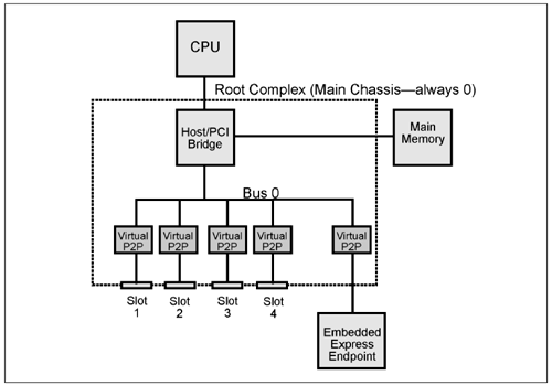
Refer to Figure 22-28 on page 862. These add-in card slots are connected to Root Ports and are not removable. These card slots do not present a problem in that the physical labeling of the slots is always correct.
Expansion Chassis—
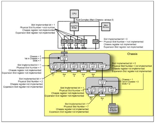
Refer to Figure 22-33 on page 869. An Expansion Chassis consists of a group of one or more buses each with card slots and the entire group can be installed in or removed from the system as a single entity. The slots within an expansion chassis are numbered sequentially and are identified by chassis number and slot number.
Chassis/Slot Numbering Registers
PCI-Compatible Chassis/Slot Numbering Register Set
"Introduction To Chassis/Slot Numbering Registers" on page 859 introduced the PCI-compatible configuration registers associated with chassis and slot numbering:
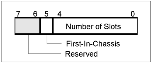
The Chassis Number register (see Figure 22-27 on page 859 and Table 22-22 on page 859). The configuration software assigns a non-zero chassis number to each upstream bridge that implements the Slot Numbering capability register set and that has a non-zero value in its Expansion Slot register (indicating the number of slots implemented within the chassis). The Expansion Slot register (see Figure 22-29 on page 864 and Table 22-23 on page 864). The Expansion Slot register is preloaded with the indicated information by hardware before the configuration software is executed. As an example, the bridge could sample a set of strapping pins on the trailing-edge of reset to determine the contents of the Expansion Slot register. A bridge may implement the Chassis/Slot numbering registers and yet may not have any expansion slots on its secondary bus. 0 indicates that no slots are implemented on the downstream side of the bridge.
Express-Specific Slot-Related Registers
In addition to these PCI-compatible registers, the following PCI Express-specific configuration registers are also involved in the process:
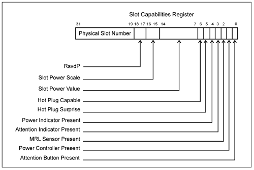
The Slot Implemented bit in the PCI Express Capabilities register (see Figure 22-31 on page 865). This bit is only implemented in the bridge to a Root Port or to a downstream switch port. If this bit is hardwired to one, this indicates that the downstream port is connected to an add-in slot rather than to an embedded device or to a disabled link. The Physical Slot Number field in the PCI Express Slot Capability register (see Figure 22-30 on page 865). This hardware initialized field indicates the physical slot number attached to this Port. The assigned slot number must be globally unique within this chassis. This field must be set to 0 for a port that is connected to a device that is either integrated on the system board or within the same silicon as the Switch device or the Root Port.
The Chassis and Expansion Slot registers must be implemented in each upstream bridge in an expansion chassis that has expansion slots on its secondary bus.
Table 22-23. Expansion Slot Register Bit Assignment|
7:6 | Reserved.
Read-only and must always return zero when read. | 5 | First-In-Chassis bit.
This bit must be set to one in the first upstream bridge within each expansion chassis. This is defined as follows:
If there is only one expansion chassis and it contains only one upstream bridge with slots on its secondary side, that bridge is the First-In-Chassis. If an expansion chassis contains a hierarchy of bridges springing from one parent upstream bridge (see Figure 22-33 on page 869), the parent upstream bridge is First-In-Chassis, while the other upstream bridges will have the First-In-Chassis bit cleared to zero.
| 4:0 | Number of Expansion Slots on bridge's secondary bus. If there aren't any expansion slots on the bridge's secondary bus, this field must be hardwired to zero. |
Two Examples
First Example
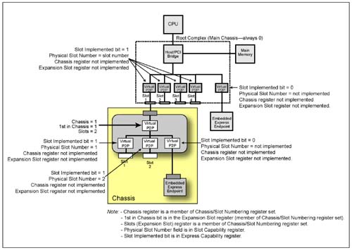
Figure 22-32 on page 867 illustrates a system wherein:
The Root Complex has four Root Ports that are connected to add-in slot connectors, and one Root Port connected to an embedded device. With the exception of the Root Port that is connected to an embedded device, in each of the Root Port bridges: - Slot Implemented bit = 1 (hardware in initialized). - Physical Slot Number = the respective slot's hardware-assigned slot number (hardware in initialized). - The Chassis register is not implemented. - The Expansion Slot register is not implemented.
The Root Port that is connected to the embedded device contains the following information: - Slot Implemented bit = 0 (hardware in initialized). - Physical Slot Number = not implemented. - Chassis register not implemented. - Expansion Slot register not implemented.
A chassis is connected to add-in slot connector number one. In the upstream bridge of the chassis: - The Chassis register in the chassis' upstream port is set to 01h by the configuration software. - The First In Chassis bit is set to one (hardware in initialized). - The upstream bridge's Expansion Slot register contains the value 2 (hardware in initialized) indicating that the chassis implements 2 add-in slot connectors on the downstream side of the bridge.
In each of the chassis' downstream port bridges: - Slot Implemented bit = 1 (hardware in initialized). - Physical Slot Number = the respective slot's hardware-assigned slot number (hardware in initialized). - The Chassis register is not implemented. - The Expansion Slot register is not implemented.
Second Example
Figure 22-33 on page 869 illustrates an example wherein:
The Root Complex has four Root Ports that are connected to add-in slot connectors, and one Root Port connected to an embedded device. With the exception of the Root Port that is connected to an embedded device, in each of the Root Port bridges: - Slot Implemented bit = 1 (hardware in initialized). - Physical Slot Number = the respective slot's hardware-assigned slot number (hardware in initialized). - The Chassis register is not implemented. - The Expansion Slot register is not implemented.
The Root Port that is connected to the embedded device contains the following information: - Slot Implemented bit = 0 (hardware in initialized). - Physical Slot Number = not implemented. - Chassis register not implemented. - Expansion Slot register not implemented.
A chassis is connected to add-in slot connector number one. In the upstream bridge of the chassis: - The Chassis register in the chassis' upstream port is set to 01h by the configuration software. - The First In Chassis bit is set to one (hardware in initialized). - The upstream bridge's Expansion Slot register contains the value 7 (hardware in initialized) indicating that the chassis implements 7 add-in slot connectors on the downstream side of the bridge.
In the bridge of each of the downstream switch ports that are connected to slots 1-through-5: - Slot Implemented bit = 1 (hardware in initialized). - Physical Slot Number = the respective slot's hardware-assigned slot number (hardware in initialized). - The Chassis register is not implemented. - The Expansion Slot register is not implemented.
In the bridge of the left-most downstream port on the same bus as slots 1-through-5: - Slot Implemented bit = 0 (hardware in initialized). - Physical Slot Number = not implemented. - Chassis register not implemented. - Expansion Slot register not implemented.
In the upstream bridge of the lower switch within the chassis: - The Chassis register in the chassis' upstream port is set to 01h by the configuration software. - The First In Chassis bit is cleared to zero (hardware in initialized). - The upstream bridge's Expansion Slot register contains the value 2 (hardware in initialized) indicating that the chassis implements 2 add-in slot connectors on the downstream side of this bridge.
In the bridge of each of the downstream ports beneath the upstream bridge: - Slot Implemented bit = 1 (hardware in initialized). - Physical Slot Number = the respective slot's hardware-assigned slot number (hardware in initialized). - The Chassis register is not implemented. - The Expansion Slot register is not implemented.
 |

