Header Type 1
General
Figure 22-13 on page 803 illustrates the layout of a PCI-to-PCI bridge's configuration header space.
Header Type 1 Registers Compatible With PCI
The Header Type 1 PCI configuration registers that are implemented and used identically in both PCI and PCI Express are:
Vendor ID register. Device ID register. Revision ID register. Class Code register. Header Type register. BIST register. Capabilities Pointer register. Subordinate Bus Number register. Secondary Bus Number register. Primary Bus Number register. IO Base, Limit and Upper registers. Memory Base and Limit registers. Expansion ROM Base Address register.
The sections that follow provide a description of each of these registers.
Header Type 1 Registers Incompatible With PCI
In a Header Type 1 bridge PCI Express function, the definitions of the following configuration registers in the function's PCI-compatible configuration space differ from the PCI spec's definition of the respective register definitions:
Command Register Status Register Cache Line Size Register Master Latency Timer Register Interrupt Line Register Interrupt Pin Register Base Address Registers Secondary Latency Timer register. Secondary Status register. Prefetchable Memory Base, Limit, and Upper registers. Bridge Control register.
The sections that follow define the implementation/usage differences of these registers. For a full description of their implementation in a PCI-to-PCI bridge function, refer to the MindShare book entitled PCI System Architecture, Fourth Edition (published by Addison-Wesley). For a full description their implementation in a PCI-X to PCI-X bridge function, refer to the MindShare book entitled PCI-X System Architecture, First Edition (published by Addison-Wesley).
Terminology
Before proceeding, it's important to define some basic terms associated with an actual or a virtual PCI-to-PCI bridge. Each PCI-to-PCI bridge is connected to two buses, referred to as its primary and secondary buses:
Downstream.
When a transaction is initiated and is passed through one or more PCI-to-PCI bridges flowing away from the host processor, it is said to be moving downstream.
Upstream.
When a transaction is initiated and is passed through one or more PCI-to-PCI bridges flowing towards the host processor, it is said to be moving upstream.
Primary bus.
PCI bus that is directly connected to the upstream side of a bridge.
Secondary bus.
PCI bus that is directly connected to the downstream interface of a PCI-to-PCI bridge.
Subordinate bus.
Highest-numbered PCI bus on the downstream side of the bridge.
Bus Number Registers
PCI-Compatible registers. Mandatory.
Introduction
Each PCI-to-PCI bridge must implement three mandatory bus number registers. All of them are read/writable and are cleared to zero by reset. During configuration, the configuration software initializes these three registers to assign bus numbers. These registers are:
the Primary Bus Number register. the Secondary Bus Number register. the Subordinate Bus Number register.
The combination of the Secondary and the Subordinate Bus Number register values defines the range of buses that exists on the downstream side of the bridge. The information supplied by these three registers is used by the bridge to determine whether or not to pass a packet through to the opposite interface.
Primary Bus Number Register
PCI-Compatible register. Mandatory. Located in Header byte zero of dword six. The Primary Bus Number register is initialized by software with the number of the bus that is directly connected to the bridge's primary interface. This register exists for three reasons:
To route Completion packets. To route a Vendor-defined message that uses ID-based routing.
To route a PCI Special Cycle Request that is moving upstream.
A bridge that connects a PCI Express link to a PCI or PCI-X bus receives a Special Cycle Request (as defined in the PCI spec) on its secondary interface. A Special Cycle Request is a request to perform a Special Cycle transaction on the destination PCI or PCI-X bus. The request takes the form of a Type 1 Configuration write request packet (see Figure 20-8 on page 734) wherein the destination ID has the following characteristics: - All ones in the Device Number and Function Number fields, and - All zeros in the Register Number and Extended Register Number fields.
If the destination bus number in the request packet matches the value in the Primary Bus Number register and the other fields are as stated above, the request is converted into a Special Cycle transaction on the primary bus and the write data is delivered as the message in the transaction's Data Phase. If it doesn't match the bridge's Primary Bus Number register and it's outside the range of buses defined by the bridge's Secondary Bus Number and Subordinate Bus Number registers, the bridge accepts the packet (the target bus is not on the downstream side of the bridge and therefore it must be passed upstream). The bridge accepts the packet and passes it to its opposite interface.
Secondary Bus Number Register
PCI-Compatible register. Mandatory. Located in Header byte one of dword six. The Secondary Bus Number register is initialized by software with the number of the bus that is directly connected to the bridge's secondary interface. This register exists for three reasons:
When a Special Cycle Request is latched on the primary side, the bridge uses this register (and, possibly, the Subordinate Bus Number register) to determine if it should be passed to the bridge's secondary interface as either a PCI Special Cycle transaction (if the bus connected to the secondary interface is the destination PCI or PCI-X bus) or as is (i.e., as a Type 1 configuration write request packet). When a Type 1 Configuration transaction (read or write and not a PCI Special Cycle Request) is latched on the primary side, the bridge uses this register (and, possibly, the Subordinate Bus Number register) to determine if it should be passed to the bridge's secondary interface as either a Type 0 configuration transaction (if the bus connected to the secondary interface is the destination PCI or PCI-X bus) or as is (i.e., as a Type 1 configuration write request packet). When a Completion packet is latched on the primary side, the bridge uses this register (and, possibly, the Subordinate Bus Number register) to determine if it should be passed to the bridge's secondary interface.
Subordinate Bus Number Register
PCI-Compatible register. Mandatory. Located in Header byte two of dword six. The Subordinate Bus Number register is initialized by software with the number of the highest-numbered bus that exists on the downstream side of the bridge. If there are no PCI-to-PCI bridges on the secondary bus, the Subordinate Bus Number register is initialized with the same value as the Secondary Bus Number register.
Bridge Routes ID Addressed Packets Using Bus Number Registers
When one of the bridge's interfaces latches a Completion packet, an ID-routed Vendor-defined message, or a PCI Special Cycle request, it uses its internal bus number registers to decide whether or not to accept the packet and pass it to the opposite bridge interface:
The routing of PCI Special Cycle requests was described in the previous sections. When the bridge latches a Completion packet or an ID-routed Vendor-defined message on its primary interface, it compares the Bus Number portion of destination ID to its Secondary Bus Number and Subordinate Bus Number register values. If the target bus number falls within the range of buses defined by the bridge's Secondary Bus Number and Subordinate Bus Number registers, the bridge accepts the packet and passes it to its opposite interface. When the bridge latches a Completion packet or an ID-routed Vendor-defined message on its secondary interface, it compares the Bus Number portion of the destination ID to its Primary Bus Number register. - If it matches, the bridge accepts the packet and passes it to the primary interface. - If it doesn't match the bridge's Primary Bus Number register and it's outside the range of buses defined by the bridge's Secondary Bus Number and Subordinate Bus Number registers, the bridge accepts the packet (the target bus is not on the downstream side of the bridge and therefore it must be passed upstream) and passes it to its primary interface. - If the destination bus falls within the range of buses defined by the bridge's Secondary Bus Number and Subordinate Bus Number registers, then the target bus is on the downstream side of the bridge. The bridge therefore does not accept the packet.
These registers are also used to route Type 1 configuration packets.
Vendor ID Register
PCI-Compatible register. Mandatory. See "Vendor ID Register" on page 773.
Device ID Register
PCI-Compatible register. Mandatory. See "Device ID Register" on page 773.
Revision ID Register
PCI-Compatible register. Mandatory. See "Revision ID Register" on page 773.
Class Code Register
PCI-Compatible register. Mandatory. Refer to Figure 22-2 on page 775. The Class field in the Class Code register of a Virtual PCI-to-PCI bridge, or a PCI Express bridge to a PCI or PCI-X bus will contain the value 06h (see Table 22-1 on page 775), the SubClass field will contain the value 04h (see Table 8 on page 1023), and the Programming Interface Byte will contain 00h.
Header Type Register
PCI-Compatible register. Mandatory. Refer to "Header Type Register" on page 777. The Header Type field in the Header Type register of a Virtual PCI-to-PCI bridge, or a PCI Express bridge to a PCI or PCI-X bus will be 01h, thereby indicating the register layout shown in Figure 22-13 on page 803.
BIST Register
PCI-Compatible register. Optional. Refer to "BIST Register" on page 778.
Capabilities Pointer Register
PCI-Compatible register. Mandatory. Refer to "Capabilities Pointer Register" on page 779.
Basic Transaction Filtering Mechanism
PCI devices that reside on the downstream side of a PCI-to-PCI bridge may incorporate internal memory (mapped into memory space) and/or an internal, device-specific register set mapped into either IO or memory-mapped IO space. The configuration program automatically detects the presence, type and address space requirements of these devices and allocates space to them by programming their address decoders to recognize the address ranges it assigns to them.
The configuration program assigns all IO devices that reside behind a PCI-to-PCI bridge mutually-exclusive address ranges that are blocked together within a common overall range of IO locations. The PCI-to-PCI bridge is then programmed to pass any IO transactions detected on the primary side of the bridge to the secondary side if the target address is within the range associated with the community of IO devices that reside behind the bridge. Conversely, any IO transactions detected on the secondary side of the bridge are passed to the primary side if the target address is outside the range associated with the community of IO devices that reside on the secondary side (because the target device doesn't reside on the secondary side, but may reside on the primary side).
All memory-mapped IO devices (i.e., non-prefetchable memory) that reside behind a PCI-to-PCI bridge are assigned mutually-exclusive memory address ranges within a common block of memory locations. The PCI-to-PCI bridge is then programmed to pass any memory-mapped IO transactions detected on the primary side of the bridge to the secondary side if the target address is within the range associated with the community of memory-mapped IO devices that reside behind the bridge. Conversely, any memory-mapped IO transactions detected on the secondary side of the bridge are passed to the primary side if the target address is outside the range associated with the community of memory-mapped IO devices that reside on the secondary side (because the target device doesn't reside on the secondary side, but may reside on the primary side).
All memory devices (i.e., regular memory, not memory-mapped IO) that reside behind a PCI-to-PCI bridge are assigned mutually-exclusive memory address ranges within a common overall range of memory locations. The PCI-to-PCI bridge is then programmed to pass any memory transactions detected on the primary side of the bridge to the secondary side if the target address is within the range associated with the community of memory devices that reside behind the bridge. Conversely, any memory transactions detected on the secondary side of the bridge are passed to the primary side if the target address is outside the range associated with the community of memory devices that reside on the secondary side (because the target device doesn't reside on the secondary side, but may reside on the primary side).
The bridge itself may incorporate:
The bridge must incorporate programmable address decoders for these devices.
Bridge's Memory, Register Set and Device ROM
Introduction
A PCI-to-PCI bridge designer may choose to incorporate the following entities within the bridge:
A set of internal, device-specific registers that are used to control the bridge's operational characteristics or check its status. These registers are outside the scope of the PCI specification. A memory buffer within the bridge. A device ROM that contains a device driver for the bridge.
The register set must be mapped into memory or IO address space (or both). The designer implements one or two Base Address Registers (programmable address decoders) for this purpose.
If there is a device ROM within the bridge, the designer must implement an Expansion ROM base address register used by configuration software to map the ROM into memory space.
Likewise, if the bridge incorporates a memory buffer, the design must include a Base Address Register used to assign a base address to the memory.
Base Address Registers
Differs from PCI. Optional. Only necessary if the bridge implements a device-specific register set and/or a memory buffer.
Located in Header dwords four and five. If the designer doesn't implement any internal, device-specific register set or memory, then these address decoders aren't necessary. These Base Address Registers are used in the same manner as those described for a non-bridge PCI function (see "Base Address Registers" on page 792). If implemented, both may be implemented as memory decoders, both as IO decoders, one as memory and one as IO, or only one may be implemented as either IO or memory.
If a BAR is implemented as a memory BAR with the prefetchable bit set to one, it must be implemented as a 64-bit memory BAR and would therefore consume both dwords four and five.
Expansion ROM Base Address Register
PCI-Compatible register. Optional. Only necessary if the bridge implements a bridge-specific device ROM. Located in Header dword 14. This register is optional (because there may not be a device ROM incorporated within the bridge). The format and usage of this register is precisely the same as that described for a non-bridge PCI function (see "Expansion ROM Base Address Register" on page 783).
Bridge's IO Filter
PCI-Compatible registers. Optional.
Introduction
There is no requirement for a bridge to support devices that reside in IO space within or behind the bridge. For this reason, implementation of the IO decode-related configuration registers is optional.
When the bridge detects an IO transaction initiated on either of its bus interfaces, it must determine which of the following actions to take:
Ignore the transaction because the target IO address isn't located on the other side of the bridge, nor is it targeting an IO location embedded within the bridge itself. When the target IO address is one of the bridge's internal IO registers, the Requester is permitted to access the targeted internal register and the transaction is not passed through the bridge. When the target IO location is located on the other side of the bridge, the transaction is passed through the bridge and is initiated on the opposite bus.
The optional configuration registers within the bridge that support this "filtering" capability are:
Base Address Registers.
If present, the Base Address Register or registers can be designed as IO or memory decoders for an internal register set or memory.
IO Base and IO Limit registers.
If the bridge supports IO space on the downstream side of the bridge, the IO Base register defines the start address and the IO Limit register defines the end address of the range to recognize and pass through to the secondary bus.
IO Extension registers (IO Base Upper 16-Bits and IO Limit Upper 16-Bits registers).
If the bridge supports a 4GB (rather than a 64KB) IO address space on the downstream side of the bridge (as indicated in the IO Base and IO Limit registers), the combination of the IO Base and the IO Base Upper 16 Bits registers define the start address, and the combination of the IO Limit and the IO Limit Upper 16-Bits registers define the end address of the range to recognize and pass to the secondary side.
The sections that follow describe each of these scenarios.
Bridge Doesn't Support Any IO Space Behind Bridge
Assume that a bridge doesn't support any devices that reside in IO space on the downstream side of the bridge. In other words, it doesn't recognize any IO addresses as being implemented behind the bridge and therefore ignores all IO transactions detected on its primary bus. In this case, the bridge designer does not implement the optional IO Base, IO Limit, or IO Extension registers (i.e., IO Base Upper 16-bits and IO Limit Upper 16-Bits registers).
The bridge ignores all IO request packets detected on the primary bus (other than transactions that may target an optional set of bridge-specific registers contained within the bridge itself).
Any IO transactions detected on the bridge's secondary bus would be claimed and passed through to the primary bus in case the target IO device is implemented somewhere upstream of the bridge.
Bridge Supports 64KB IO Space Behind Bridge
Assume that a bridge is designed to support IO transactions initiated on the primary bus that may target locations within the first 64KB of IO space (IO locations 00000000h through 0000FFFFh) on the secondary side of the bridge. It ignores any primary side IO accesses over the 64KB address boundary. In other words, the bridge supports a 64KB IO space, but not a 4GB IO space on the secondary side of the bridge.
In this case, the bridge designer must implement the IO Base and the IO Limit registers, but does not implement the IO Extension registers (i.e., the IO Base Upper 16-Bits and the IO Limit Upper 16-Bits registers).
The IO Base and IO Limit register pair comprise the global IO address decoder for all IO targets that reside on the secondary side of the bridge:
Before the registers are initialized by the configuration software, they are first read from to determine whether they support 64KB or a 4GB of IO space on the secondary side of the bridge. In this scenario, assume that the registers are hardwired to indicate that the bridge only supports a 64KB IO space. The configuration software then walks the secondary bus (and any subordinate buses it discovers) and assigns to each IO decoder it discovers an exclusive IO address range within the first 64KB of IO space. The sub-ranges assigned to the devices are assigned in sequential blocks to make efficient use of IO space. The IO Base and Limit register pair are then initialized by the startup configuration software with the start and end address of the IO range that all IO devices that were discovered behind the bridge (on the secondary and on any subordinate buses) have been programmed to reside within. In this case, since the bridge only supports the first 64KB of IO space, the defined range will be a subset of the first 64KB of IO space. After they have been initialized, these two registers provide the bridge with the start and the end address of the IO address range to recognize. After they have been initialized, these two registers provide the bridge with the start and the end address of the IO address range to recognize for passing IO transactions through the bridge.
The bridge only supports the lower 64KB of IO space, but the IO address decoder comprised of the IO Base and Limit registers must perform a full IO address decode of address bits [31:2] to determine whether or not to accept an IO access on the primary bus and pass it to the secondary bus.
The format of the IO Base and IO Limit registers are illustrated in Figure 22-14 on page 815 and Figure 22-15 on page 815. Both registers have the same format:
the upper hex digit, bits [7:4], defines the most-significant hex digit of a 16-bit IO address; the lower hex digit, bits [3:0], defines whether the bridge performs a 16-bit or 32-bit IO address decode.
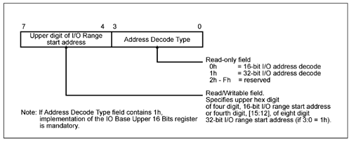
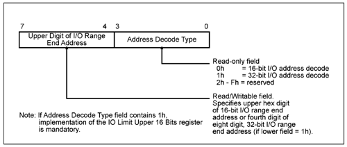
In the scenario under discussion, the lower hex digit of both registers is hardwired with the value 0h, indicating that it performs a 16-bit IO address decode and therefore only supports addresses within the first 64KB of IO space.
Assume that the configuration software programs the upper digit of the IO Base register with the value 2h and the upper digit of the IO Limit register with the value 3h. This indicates that the start of the IO range to recognize is 2000h and the end address is 3FFFh—an 8KB block. As another example, assume that the upper digit in the base and limit registers are both set to 3h. The IO address range to recognize is then 3000h through 3FFFh—a 4KB block. In other words, this register pair defines the start address aligned on a 4KB address boundary, and the size, also referred to as the granularity, of the defined block is in increments of 4KB.
It should be noted that, if there aren't any IO devices on the bridge's secondary side, the IO Limit register can be programmed with a numerically lower IO address than the IO Base register. The bridge will not pass any IO transactions latched on the primary side through to the secondary side, but will pass any IO transactions latched on the secondary side through to the primary side.
|
Example.
Assume that the IO base is set to 2h and the IO Limit is set to 3h. The bridge is now primed to recognize any IO transaction on the primary bus that targets an IO address within the range consisting of 2000h through 3FFFh. Refer to Figure 22-16 on page 817.
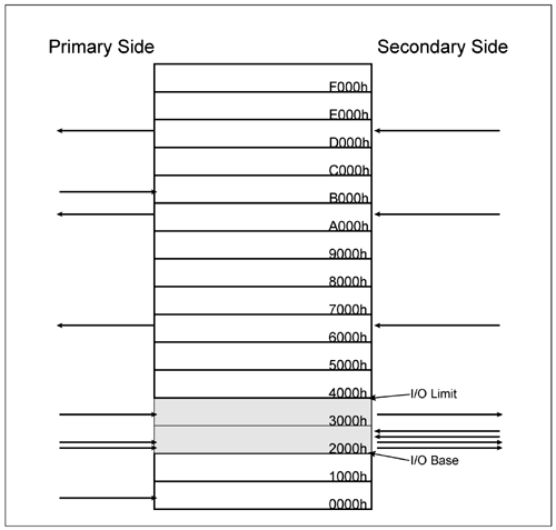
Anytime that the bridge detects an IO transaction on the primary bus with an address inside the 2000h through 3FFFh range, it accepts the transaction and passes it through (because it's within the range defined by the IO Base and Limit registers and may therefore be for an IO device that resides behind the bridge).
Anytime that the bridge detects an IO transaction on the primary bus with an address outside the 2000h through 3FFFh range, it ignores the transaction (because the target IO address is outside the range of addresses assigned to IO devices that reside behind the bridge).
Anytime that the bridge detects an IO transaction on the secondary bus with an address inside the 2000h through 3FFFh range, it ignores the transaction (because the target address falls within the range assigned to IO devices that reside on the secondary side of the bridge).
Anytime that the bridge detects an IO transaction on the secondary bus with an address outside the 2000h through 3FFFh range, it accepts the transaction and passes it through to the primary side (because the target address falls outside the range assigned to IO devices that reside on the secondary side of the bridge, but it may be for an IO device on the primary side). |
Bridge Supports 4GB IO Space Behind Bridge
Assume a bridge is designed to recognize IO transactions initiated on the primary bus that target locations anywhere within 4GB of IO space (IO locations 00000000h through FFFFFFFFh) on the downstream side of the bridge.
In this case, in addition to the IO Base and the IO Limit registers, the bridge designer must also implement the IO Extension registers—IO Base Upper 16-bits and the IO Limit Upper 16-bits registers:
The IO Base register is initialized with the fourth digit of the 32-bit start IO address. The IO Base Upper 16 bits register is initialized with the fifth through the eight digits of the 32-bit start address of the range. The IO Limit register is initialized with the fourth digit of the 32-bit end IO address. The IO Limit Upper 16 bits register is initialized with the fifth through eighth digits of the 32-bit end address of the range.
The IO Base and IO Limit register pair comprise an IO address decoder. They are used as follows:
Before the registers are initialized by the configuration software, they are read from to determine if they are capable of supporting a 64KB or a 4GB IO address space behind the bridge. In this scenario, the Address Decode Type field (see Figure 22-14 on page 815) within each of the registers is hardwired (with a value of 1h) to indicate that a 4GB IO space is supported on the secondary side. The configuration software than walks the secondary bus (and any subordinate buses it discovers beneath the secondary bus) and assigns each IO device that it discovers an exclusive IO address range within the 4GB IO space. The sub-ranges assigned to the devices are assigned in sequential blocks to make efficient use of IO space. The IO Base and IO Base Extension (i.e., the IO Base Upper 16-bits) register pair is then initialized by the startup configuration software with the upper five digits of the 4KB-aligned, 32-bit start address of the IO range that all IO devices that were discovered behind the bridge (on the secondary and on any subordinate buses) have been programmed to reside within. The IO Limit and IO Limit Extension (i.e., the IO Limit Upper 16 bits) register pair is initialized with the 4KB-aligned end address of the range that the devices occupy.
In the scenario under discussion, since the bridge supports the entire 4GB IO space, the defined range is a subset of the overall 4GB IO space. After they have been initialized, these four registers provide the bridge with the start and the end address of the IO address range to recognize.
Since the bridge supports the entire 4GB IO space, the IO address decoder comprised of the four registers (Base and Limit registers plus their Extension registers) performs an IO address decode within address bits [31:12] to determine whether or not to pass an IO access detected on the primary bus through to the secondary bus and vice versa.
The format of the IO Base and IO Limit registers was illustrated earlier in Figure 22-14 on page 815 and Figure 22-15 on page 815. In the scenario under discussion, the lower hex digit of the Base and Limit registers is hardwired with the value 1h, indicating a 32-bit IO address decode, supporting address recognition within the entire 4GB IO space. Simply put, the IO Base and IO Limit Upper 16-bits registers are used to hold the upper four digits of the start and end IO address boundaries, respectively.
Assume that the configuration software programs the registers as follows:
Upper digit of the IO Base = 2h. IO Base Upper 16-bits register = 1234h. Upper digit of the IO Limit register = 3h. IO Limit Upper 16-bits register = 1235h.
This indicates a 72KB range consisting of:
As another example, assume the following:
Upper digit of the IO Base = 3h. IO Base Upper 16-bits register = 1234h. Upper digit of the IO Limit register = 3h. IO Limit Upper 16-bits register = 1234h.
This indicates a 4KB range consisting of:
In other words, the four registers define the start address aligned on a 4KB address boundary, and the size of the defined block is an increment of 4KB.
Bridge's Prefetchable Memory Filter
Differs from PCI. Optional.
An Important Note From the Authors
Although the Express spec appears to support the concept of a bridge within a Root Complex or a Switch reading more data than is actually requested from areas of memory defined as prefetchable (see the spec statements included below), it is the opinion of the authors that a bridge within a Root Complex or a Switch will not do so. Our rationale is provided below.
In PCI
When a PCI bus master initiates a memory read transaction, it issues the start memory address but does not indicate how much data is to be read. The only exception is a single Data Phase memory read. In that case, the total amount of data to be read is represented by the Byte Enables that are presented in that Data Phase.
When the device acting as the target on the initiating bus receives the transaction request, the manner in which the request is handled depends on the device type (bridge or ultimate memory target), as well as the transaction type used by the bus master:
If device acting as the target is the ultimate target of the read: - and the memory is well-behaved, prefetchable memory, then the target may perform internal prefetches (i.e., read-aheads) and queue up data to be supplied to the requester if the transaction ends up asking for the data. This is to enhance performance. If the transaction ends without all of the prefetched data being asked for, the remaining data in the target's read-ahead buffer should be discarded (unless the target can guarantee the continued freshness of the data). - and the memory is not prefetchable memory (e.g., it's a memory-mapped IO register set), then the memory target must wait until the Byte Enables are presented in each Data Phase and only read and supply the requested bytes. No prefetching is permitted.
If the device acting as the target is a bridge in the path to the target, the bridge latches the request and issues a Retry to the initiating master: - and the transaction type is Memory Read, there are two possibilities: - If the memory address is within a range defined as prefetchable memory, the bridge may turn the read into a burst read when it initiates the request on the other side of the bridge and prefetch data into a bridge buffer. When the original master then retries the transaction, the bridge sources data from the fast read-ahead buffer yielding better performance. If the master ultimately doesn't consume all of the data, it is discarded by the bridge. - and the memory is not prefetchable memory (e.g., it's a memory-mapped IO register set), then no prefetching by the bridge is permitted when it re-initiates the read on the opposite side of the bridge.
- and the transaction type is Memory Read Line (MRL), this tells the bridge that the master has specific knowledge that the memory range from the transaction's start address up to the end of the addressed line of memory space is prefetchable memory. Even if the bridge's prefetchable memory range registers indicate this is not prefetchable memory, the bridge may turn the read into a burst read when it initiates the request on the other side of the bridge and prefetch data up to the end of the current line into a bridge buffer. When the original master then retries the transaction, the bridge sources data from the fast read-ahead buffer yielding better performance. If the master ultimately doesn't consume all of the data, it is discarded by the bridge. - and the transaction type is Memory Read Multiple (MRM), this tells the bridge that the master has specific knowledge that the memory range from the transaction's start address and up to the end of the line immediately following the addressed line of memory space is prefetchable memory. Even if the bridge's prefetchable memory range registers indicate this is not prefetchable memory, the bridge may turn the read into a burst read when it initiates the request on the other side of the bridge and prefetch data across cache line boundaries into a bridge buffer. When the original master then retries the transaction, the bridge sources data from the fast read-ahead buffer yielding better performance. If the master ultimately doesn't consume all of the data, it is discarded by the bridge.
In PCI Express
When a PCI Express Requester issues a memory read request, it indicates the exact amount of data it wishes to read:
The First DW Byte Enable field in the request packet header indicates the byte(s) to be read from the first dword. The Length field in the request packet header indicates the overall number of dwords in the transfer. The Last DW Byte Enable field in the request packet header indicates the byte(s) to be read from the last dword.
Since the exact amount of requested data is known at the onset of a memory read request, there is no reason for prefetching to achieve better performance (as there is in PCI).
Spec References To Prefetchable Memory
The following Express spec 1.0a references represent all of its references to prefetching:
Page 33, line 5:
"A PCI Express Endpoint requesting memory resources through a BAR must set the BAR's Prefetchable bit unless the range contains locations with read side-effects or locations in which the device does not tolerate write merging".
Page 33, line 8:
"For a PCI Express Endpoint, 64-bit addressing must be supported for all BARs that have the prefetchable bit set. 32-bit addressing is permitted for all BARs that do not have the prefetchable bit set."
Page 52, line 13:
"For each bit of the Byte Enables fields: a value of 0b indicates that the corresponding byte of data must not be written or, if non prefetchable, must not be read at the Completer."
Page 54, line 9:
"This is really just a specific case of the rule that in a non-prefetchable space, non-enabled bytes must not be read at the Completer."
Page 265, line 26:
"For example, if a Read is issued to prefetchable memory space and the Completion returns with a Unsupported Request Completion Status, perhaps due to a temporary condition, the initiator may choose to reissue the Read Request without side effects."
Page 326, line 5:
"A PCI Express Endpoint requesting memory resources through a BAR must set the BAR's Prefetchable bit unless the range contains locations with read side-effects or locations in which the device does not tolerate write merging. It is strongly encouraged that memory-mapped resources be designed as prefetchable whenever possible. PCI Express devices other than legacy Endpoints must support 64-bit addressing for any Base Address register that requests prefetchable memory resources".
Page 328, line 1:
"A PCI Express Endpoint requesting memory resources through a BAR must set the BAR's Prefetchable bit unless the range contains locations with read side-effects or locations in which the device does not tolerate write merging. It is strongly encouraged that memory-mapped resources be designed as prefetchable whenever possible. PCI Express devices other than legacy Endpoints must support 64-bit addressing for any Base Address register that requests prefetchable memory resources."
Page 329:
"The Prefetchable Memory Base and Prefetchable Memory Limit registers must indicate that 64-bit addresses are supported, as defined in PCI Bridge 1.1." Please note that this not so. Section 3.2.5.10 in the 1.1 bridge spec states "The Prefetchable Base Upper 32 Bits and Prefetchable Limit Upper 32 Bits registers are optional extensions to the Prefetchable Memory Base and Prefetchable Memory Limit registers."
Characteristics of Prefetchable Memory Devices
While the Memory Base and Limit registers are mandatory (to support memory-mapped IO behind the bridge). The Prefetchable Memory Base and Limit registers (and their extensions) are optional (there is no requirement for a bridge to support prefetchable memory on its downstream side). The PCI-to-PCI bridge specification recognizes the fact that while both groups are mapped into memory address space, memory devices and memory-mapped IO devices can have distinctly different operational characteristics.
An optional set of registers are provided in the bridge's configuration space that permit the configuration software to define the start and end address of the prefetchable memory space that is occupied by well-behaved memory devices behind the bridge. A mandatory register pair permits the configuration software to define the start and end address of the memory-mapped IO space that is occupied by well-behaved memory devices behind the bridge.
Multiple Reads Yield the Same Data
A well-behaved memory device always returns the same data from a location no matter how many times the location is read from. In other words, reading from a memory device doesn't in any way alter the contents of memory. This is one of the characteristics of a prefetchable memory target.
Byte Merging Permitted In the Posted Write Buffer
A bridge incorporates a posted-write buffer that quickly absorbs data to be written to a memory device on the other side of the bridge. Since the initiating Requester is able to immediately complete a memory write and doesn't have to delay until the write to the memory device has actually been completed, posting yields better performance during memory write operations. The bridge would ensure that, before any subsequent memory read is permitted to propagate through the bridge, the bridge would flush its posted-write buffer to the memory device. Byte merging is permitted in a bridge's posted memory write buffer when handling writes to prefetchable memory (for more information, refer to "Byte Merging" on page 801).
Characteristics of Memory-Mapped IO Devices
Memory-mapped IO devices exhibit a different set of operational characteristics.
Read Characteristics
Performing a memory read from a memory-mapped IO location often has the effect of altering the contents of the location. As examples, one of the following may be true:
The location may be occupied by a memory-mapped IO status port. Reading from the location causes the IO device to deassert any status bits that were set in the register (on the assumption that they've been read and will therefore be dealt with by the device driver). If the read was caused by a prefetch and the prefetched data is never actually read by the device driver, then status information has just been discarded. The location may be the front-end of a FIFO data buffer. Performing a read from the location causes the delivery of its current contents and the next data item is then automatically placed in the location by the IO device. The device assumes that the first data item has just been read by the device driver and sets up the next data item in the FIFO location. If the read was caused by a prefetch and the prefetched data is never actually read by the device driver, then the data has just been discarded.
Reads within an area of memory space occupied by memory-mapped IO devices must never result in prefetching by a bridge. A mandatory set of registers are provided that permit the configuration software to define the start and end address of the memory space that is occupied by memory-mapped IO devices that reside on the bridge's secondary side.
Write Characteristics
See "Byte Merging" on page 801.
Determining If Memory Is Prefetchable or Not
The configuration software determines that a memory target supports prefetching by testing the state of the Prefetchable attribute bit in the memory target's Base Address Register (see "Base Address Registers" on page 792 and "Prefetchable Attribute Bit" on page 795).
Prefetchable = 1 indicates that the memory is prefetchable. The memory target must be mapped into Prefetchable memory space using the bridge's Prefetchable Base and Limit configuration registers ( if they are implemented). Prefetchable = 0 indicates that it's not. In this case, the memory target must be mapped into memory-mapped IO space using the Memory Base and Limit registers.
Bridge Support For Downstream Prefetchable Memory Is Optional
If the bridge does not support Prefetchable memory on its secondary side, the Prefetchable Memory Base and Limit registers must be implemented as read-only registers that return zero when read, and the Prefetchable Memory Base and Prefetchable Memory Limit registers are not implemented.
Must Support > 4GB Prefetchable Memory On Secondary Side
Whether or not a bridge supports prefetchable memory on the bridge's downstream side is optional. If the designer chooses to support this capability, then the following registers must be implemented to define the start and end address of the memory range occupied by prefetchable memory devices on the downstream side of the bridge:
These two registers are used to define the start (base) and end (limit) address of the memory range and are illustrated in Figure 22-17 on page 827 and Figure 22-18 on page 828. Any address within the lower 4GB can be specified. The start address is 1MB-aligned and the size of the range is specified in 1MB increments. The Express spec states that all memory BARs for prefetchable memory must be implemented as 64-bit registers (see Figure 22-11 on page 797). To support this, the extensions to Base and Limit registers must also be implemented:
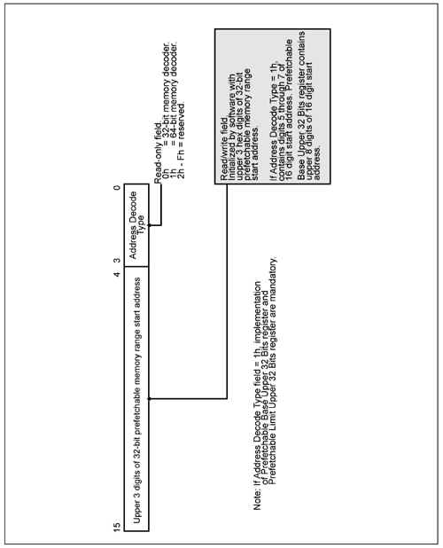
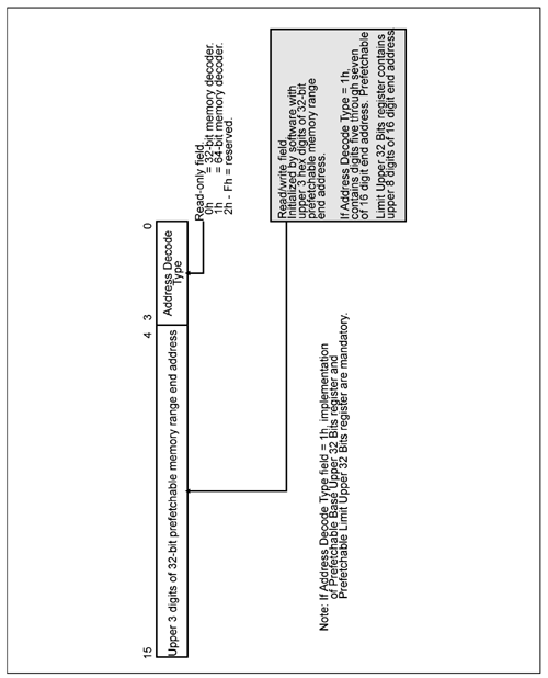
The 4-bit Address Decode Type field in the Base and Limit registers is hardwired to indicate that the extension registers are present.
The configuration software walks the secondary bus and any buses subordinate to the bridge and assigns each Prefetchable memory target a sub-range in a global overall range within the 264 memory space. After completing the address assignment process, the software then writes the upper eight hex digits of the range's 64-bit start address into the Prefetchable Memory Base Upper register and the next three hex digits into the upper three digits of the Base register. The upper eight hex digits of the range's 64-bit end address is written into the Prefetchable Memory Limit Upper register and the next three hex digits into the upper three digits of the Limit register.
As an example, assume that these four registers are set as follows:
FF00000h is written into the Prefetchable Memory Base Upper 32-bits register. 123h is written into the upper three digits of the Base register. FF000000h is written into Prefetchable Memory Limit Upper 32-bits register. 124h is written into the upper three digits of the Limit register.
This defines the Prefetchable memory address range as the 2MB range from FF00000012300000h through FF000000124FFFFFh. As another example, assume they are programmed as follows:
00000230h is written into the Prefetchable Memory Base Upper 32-bits register. 222h written into the upper three digits of the Base register. 00000230h is written into Prefetchable Memory Limit Upper 32-bits register. 222h written into the upper three digits of the Limit register.
This defines the Prefetchable memory address range as the 1MB range from 0000023022200000h through 00000230222FFFFFh.
Rules for Bridge Prefetchable Memory Accesses
The following rules apply to Prefetchable memory:
Bridge support for Prefetchable memory on its secondary side is optional. If the bridge does not support Prefetchable memory on its secondary side, the Prefetchable Memory Base and Limit registers must be implemented as read-only registers that return zero when read. If the bridge does support prefetchable memory on its downstream side, it must implement the Prefetchable Memory Base and Limit registers, as well as the Prefetchable Memory Base and Limit Upper 32-bits registers (as indicated by hardwiring the first digit in the Base and Limit registers to a value of 1h). Memory transactions are forwarded from the primary to the secondary bus if the address is within the range defined by the Prefetchable Memory Base and Limit registers or that defined by the Memory Base and Limit registers (for memory-mapped IO). Memory transactions are forwarded from the secondary to the primary bus when the address is outside the ranges defined by the extended Prefetchable Memory Base and Limit registers and the Memory Base and Limit registers (for memory-mapped IO). When 264 memory is supported on the downstream side of the bridge, transactions targeting addresses within the address range specified by the Prefetchable Memory Base and Limit registers (and their extensions) are permitted to cross the 4GB boundary. The bridge designer must support memory access requests above the 4GB address boundary received by its downstream interface. Prior to the 1.1 PCI-to-PCI bridge spec, it was optional on both sides. This was changed to ensure that Requesters on the secondary side can access main memory above the 4GB address boundary. Assume that the bridge supports Prefetchable memory anywhere in 264 memory space on the downstream side, but the configuration software maps all Prefetchable memory behind the bridge below the 4GB boundary. In this case, the upper extensions of the Prefetchable Base and Limit registers must be set to zero and the bridge does not respond to memory access requests above the 4GB address boundary received on the upstream interface. Those received by the bridge's downstream interface would be passed to the upstream interface (in case the Requester is addressing main memory above the 4GB boundary). Assume that the bridge supports Prefetchable memory anywhere in 264 memory space on the downstream side and that the configuration software maps all Prefetchable memory on the downstream side above the 4GB boundary. In this case, the upper extensions of the Prefetchable Base and Limit registers contain non-zero values and the bridge responds only to prefetchable memory access requests received on its upstream interface that are above the 4GB address boundary and within the defined prefetchable memory address range. Assume that the bridge supports Prefetchable memory anywhere in 264 memory space behind the bridge and that the configuration software maps the Prefetchable memory on the bridge's downstream side into a space that straddles the 4GB boundary. In this case, the extension to the Prefetchable Base register is set to zero and the extension to the Limit register contains a non-zero value. When a memory request with an address below the 4GB boundary is detected on either interface, the bridge compares the address only to the Prefetchable Memory Base register. If the address is  the start address specified in the register, the address is in range. When a memory request with an address above the 4GB boundary is detected on either interface, the bridge compares the lower 32-bits of the address to the Limit register and the Upper 32-bits of the address to the Limit Upper 32-bits register. If the address is the start address specified in the register, the address is in range. When a memory request with an address above the 4GB boundary is detected on either interface, the bridge compares the lower 32-bits of the address to the Limit register and the Upper 32-bits of the address to the Limit Upper 32-bits register. If the address is  the end address specified in the two registers, the address is in range. the end address specified in the two registers, the address is in range. The bridge may be designed to assume that all memory accesses received by its downstream interface that are passed to the primary bus are prefetchable. This assumes that the destination of all memory reads traveling upstream is system memory (which is prefetchable). If a bridge makes this assumption, it must implement a device-specific bit in its configuration space that allows this ability to be disabled. Memory writes received by either of the bridge's interfaces are accepted into the bridge's downstream or upstream posted memory write buffer. As described in "Byte Merging" on page 801, the bridge is permitted to perform byte merging in the buffer for writes to prefetchable memory, but not to memory-mapped IO.
Bridge's Memory-Mapped IO Filter
PCI-Compatible registers. Mandatory. The bridge designer is required to implement the Memory Base and Limit registers used to define a memory-mapped IO range. These two registers are used to define a range of memory occupied by memory-mapped IO devices that reside on the downstream side of the bridge. Figure 22-19 on page 831 and Figure 22-20 on page 831 illustrate the Memory Base and Limit registers. The lower digit of each register is hardwired to zero and the upper three digits are used to define the upper three hex digits of the eight-digit start and end addresses, respectively. Unlike the Prefetchable Base and Limit and IO Base and Limit register pairs, there are no Extension registers associated with the Memory Base and Limit register pair. This means that all memory-mapped IO devices in the system must reside in the lower 4GB of memory address space.
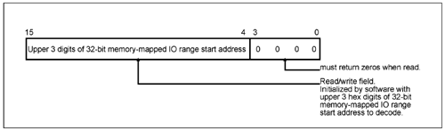
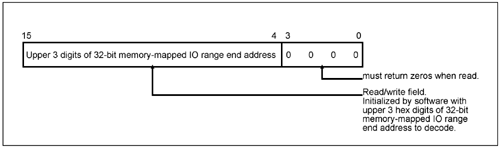
As an example, assume that the configuration software has written the following values to the Memory Base and Limit registers:
This defines a 292MB memory-mapped IO region on the downstream side of the bridge starting at 55500000h and ending at 678FFFFFh.
Bridge Command Registers
Differs from PCI. Mandatory.
Introduction
The bridge designer must implement two required command registers in the bridge's configuration Header region:
The Command register is the standard configuration Command register defined by the spec for any function. It is associated with the bridge's primary bus interface. The Bridge Control register is an extension to the standard Command register and is associated with the operation of both of the bridge's bus interfaces.
These two registers are described in the next two sections.
Bridge Command Register
Differs from PCI. Mandatory. The Command register format, pictured in Figure 22-21 on page 832, is the same as that for a non-bridge function. Some of the bits, however, have different effects. Each of the bits is described in Table 22-6 on page 833.
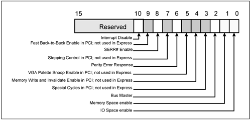
Table 22-6. Bridge Command Register Bit Assignment|
0 | RW | IO Address Space Decoder Enable.
- 0. IO transactions received at the downstream side of a bridge that are moving in the upstream direction are not forwarded and no error is reported. - 1. IO transactions received at the downstream side of a bridge that are moving in the upstream direction are forwarded from the secondary to primary side of the bridge.
| 1 | RW | Memory Address Space Decoder Enable.
| 2 | RW | Bus Master.
- Controls the ability of a Root Port or a downstream Switch Port to forward memory or IO requests in the upstream direction. - If this bit is 0, when a Root Port or a downstream Switch Port receives an upstream-bound memory request or IO request, it returns Unsupported Requests (UR) status to the requester. - This bit does not affect forwarding of Completions in either the upstream or downstream direction. - The forwarding of requests other than those mentioned above are not controlled by this bit. - Default value of this bit is 0.
| 3 | RO | Special Cycles.
Does not apply to PCI Express and must be hardwired to 0. | 4 | RO | Memory Write and Invalidate Enable.
Does not apply to PCI Express and must be hardwired to 0. | 5 | RO | VGA Palette Snoop.
Does not apply to PCI Express and must be hardwired to 0. | 6 | RW | Parity Error Response.
When forwarding a Poisoned TLP from Primary to Secondary:
The primary side must set the Detected Parity Error bit in the bridge Status register. If the Parity Error Response bit in the Bridge Control register is set, the secondary side must set the Master Data Parity Error bit in the Secondary Status register.
When forwarding a Poisoned TLP from Secondary to Primary:
The secondary side must set the Detected Parity Error bit in the Secondary Status register. If the Parity Error Response bit in the Bridge Control register is set, the primary side must set the Master Data Parity Error bit in the bridge Status register.
If the Parity Error Response bit is cleared, the Master Data Parity Error status bit in the bridge Status register is never set.
The default value of this bit is 0. | 7 | RO | Stepping Control.
Does not apply to PCI Express. Must be hardwired to 0. | 8 | RW | SERR# Enable.
When set, this bit enables the non-fatal and fatal errors detected by the bridge's primary interface to be reported to the Root Complex. The function reports such errors to the Root Complex if it is enabled to do so either through this bit or through the PCI Express specific bits in the Device Control register (see "Device Control Register" on page 905). The default value of this bit is 0. | 9 | RO | Fast Back-to-Back Enable.
Does not apply to PCI Express and must be hardwired to 0. | 10 | RW | Interrupt Disable.
Controls the ability of a bridge to generate INTx interrupt messages:
If the bridge had already transmitted any Assert_INTx emulation interrupt messages and this bit is then set, it must transmit a corresponding Deassert_INTx message for each assert message transmitted earlier.
Note that INTx emulation interrupt messages forwarded by Root and Switch Ports from devices downstream of the Root or Switch Port are not affected by this bit. The default value of this bit is 0. | 15:11 | | Reserved.
Read-only and must return zero when read. |
Bridge Control Register
Differs from PCI. Mandatory. The Bridge Control register is a required extension to the bridge's Command register and is associated with the operation of both the primary and the secondary bridge interfaces. Figure 22-22 on page 835 illustrates this register and Table 22-7 on page 836 defines its bit assignment. Bits 8 - through - 11 were first defined in the 2.2 PCI spec.
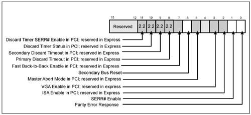
Table 22-7. Bridge Control Register Bit Assignment|
0 | RW | Parity Error Response.
When forwarding a Poisoned TLP from Primary to Secondary:
The primary side must set the Detected Parity Error bit in the bridge Status register. If the Parity Error Response bit in the Bridge Control register is set, the secondary side must set the Master Data Parity Error bit in the Secondary Status register.
When forwarding a Poisoned TLP from Secondary to Primary:
The secondary side must set the Detected Parity Error bit in the Secondary Status register. If the Parity Error Response bit in the Bridge Control register is set, the primary side must set the Master Data Parity Error bit in the bridge Status register.
If the Parity Error Response bit is cleared, the Master Data Parity Error status bit in the Secondary Status register is never set.
The default value of this bit is 0. | 1 | RW | SERR# Enable.
This bit controls the forwarding of ERR_COR (correctable errors), ERR_NONFATAL (non-fatal errors), and ERR_FATAL (fatal errors) received on the secondary side to the primary side.
Default value of this field is 0. | 2 | RO | ISA Enable.
Not used in Express and must be hardwired to zero. | 3 | RO | VGA Enable.
Not used in Express and must be hardwired to zero. | 4 | RO | Reserved.
Hardwired to zero. | 5 | RO | Master Abort Mode.
Not used in Express and must be hardwired to zero. | 6 | RW | Secondary Bus Reset.
Setting this bit to one triggers a hot reset on the Express downstream port.
Port configuration registers must not be affected, except as required to update port status.
Default value of this field is 0. | 7 | RO | Fast Back-to-Back Enable.
Not used in Express and must be hardwired to zero. | 8 | RO | Primary Discard Timeout.
Not used in Express and must be hardwired to zero. | 9 | RO | Secondary Discard Timeout.
Not used in Express and must be hardwired to zero. | 10 | RO | Discard Timer Status.
Not used in Express and must be hardwired to zero. | 11 | RO | Discard Timer SERR# Enable.
Not used in Express and must be hardwired to zero. |
Bridge Status Registers
Introduction
The bridge contains two required status registers, each of which is associated with one of the two interfaces.
Bridge Status Register (Primary Bus)
Differs from PCI. Mandatory. Refer to Figure 22-23 on page 838 and Table 22-8 on page 838. This required register is completely compatible with the Status register definition for a non-bridge function (see "Status Register" on page 788) and only reflects the status of the bridge's primary interface.
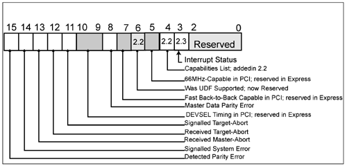
If the Capabilities List bit (bit 4) is set to one, this indicates that the bridge implements the Capability Pointer register in byte 0 of dword 13 in its configuration Header (see Figure 22-13 on page 803). For a general description of the New Capabilities, refer to "Capabilities Pointer Register" on page 779. In subsequently traversing the New Capabilities list, software may discover that the bridge implements the Slot Numbering registers. For a description of this feature, refer to "Introduction To Chassis/Slot Numbering Registers" on page 859 and "Chassis and Slot Number Assignment" on page 861.
Table 22-8. Bridge Primary Side Status Register|
3 | RO | Interrupt Status.
Indicates that the bridge itself had previously transmitted an interrupt request to its driver (that is, the function transmitted an interrupt message earlier in time and is awaiting servicing).
Note that INTx emulation interrupts forwarded by Root and Switch Ports from devices downstream of the Root or Switch Port are not reflected in this bit. The default state of this bit is 0. | 4 | RO | Capabilities List.
Indicates the presence of one or more extended capability register sets in the lower 48 dwords of the function's PCI-compatible configuration space. Since, at a minimum, all PCI Express functions are required to implement the PCI Express capability structure, this bit must be set to 1. | 5 | RO | 66MHz-Capable.
Does not apply to PCI Express and must be 0. | 7 | RO | Fast Back-to-Back Capable.
Does not apply to PCI Express and must be 0. | 8 | RW1C | Master Data Parity Error.
When forwarding a Poisoned TLP from Primary to Secondary:
The primary side must set the Detected Parity Error bit in the bridge Status register. If the Parity Error Response bit in the Bridge Control register is set, the secondary side must set the Master Data Parity Error bit in the Secondary Status register.
When forwarding a Poisoned TLP from Secondary to Primary:
The secondary side must set the Detected Parity Error bit in the Secondary Status register. If the Parity Error Response bit in the Bridge Control register is set, the primary side must set the Master Data Parity Error bit in the bridge Status register.
If the Parity Error Response bit in the Bridge Command register is cleared, the Master Data Parity Error status bit in the Secondary Status register is never set.
The default value of this bit is 0. | 10:9 | RO | DEVSEL Timing.
Does not apply to PCI Express and must be 0. | 11 | RW1C | Signaled Target Abort.
This bit is set when the bridge's primary interface completes a received request by issuing a Completer Abort Completion Status.
Default value of this field is 0. | 12 | RW1C | Received Target Abort.
This bit is set when the bridge's primary interface receives a Completion with Completer Abort Completion Status.
Default value of this field is 0. | 13 | RW1C | Received Master Abort.
This bit is set when the bridge's primary interface receives a Completion with Unsupported Request Completion Status.
Default value of this field is 0. | 14 | RW1C | Signaled System Error.
This bit is set when the bridge's primary interface sends an ERR_FATAL (fatal error) or ERR_NONFATAL (non-fatal error) message (if the SERR Enable bit in the bridge Command register is set to one).
The default value of this bit is 0. | 15 | RW1C | Detected Parity Error.
This bit is set by the bridge's primary interface whenever it receives a Poisoned TLP, regardless of the state the Parity Error Enable bit in the bridge Command register. Default value of this bit is 0. |
Bridge Secondary Status Register
Differs from PCI. Mandatory. Refer to Figure 22-24 on page 841. With the exception of the Received System Error bit, this required register is completely compatible with the Status register definition for a non-bridge function (see "Status Register" on page 788) and only reflects the status of the secondary side. It should be noted that the Capabilities List bit (bit 4) is never implemented in this register.
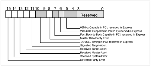
While bit 14 is the Signaled System Error bit in the primary side Status register, it is the Received System Error bit in the Secondary Status register. When set, this bit indicates that SERR# was detected asserted on the secondary side. Writing a one to it clears the bit, while a zero doesn't affect it. Reset clears this bit.
Table 22-9. Bridge Secondary Side Status Register|
5 | RO | 66MHz-Capable.
Does not apply to Express and must be 0. | 7 | RO | Fast Back-to-Back Capable.
Does not apply to PCI Express and must be 0. | 8 | RW1C | Master Data Parity Error.
When forwarding a Poisoned TLP from Primary to Secondary:
The primary side must set the Detected Parity Error bit in the bridge Status register. If the Parity Error Response bit in the Bridge Control register is set, the secondary side must set the Master Data Parity Error bit in the Secondary Status register.
When forwarding a Poisoned TLP from Secondary to Primary:
The secondary side must set the Detected Parity Error bit in the Secondary Status register. If the Parity Error Response bit in the Bridge Control register is set, the primary side must set the Master Data Parity Error bit in the bridge Status register.
If the Parity Error Response bit in the Bridge Control register is cleared, the Master Data Parity Error status bit in the Secondary Status register is never set. The default value of this bit is 0. | 10:9 | RO | DEVSEL Timing.
Does not apply to Express and must be 0. | 11 | RW1C | Signaled Target Abort.
This bit is set when the bridge's secondary interface completes a received request by issuing a Completer Abort Completion Status. Default value of this field is 0. | 12 | RW1C | Received Target Abort.
This bit is set when the bridge's secondary interface receives a Completion with Completer Abort Completion Status. Default value of this field is 0. | 13 | RW1C | Received Master Abort.
This bit is set when the bridge's secondary interface receives a Completion with Unsupported Request Completion Status. Default value of this field is 0. | 14 | RW1C | Signaled System Error.
This bit is set when the bridge's secondary interface sends an ERR_FATAL (fatal error) or ERR_NONFATAL (non-fatal error) message (if the SERR Enable bit in the Bridge Control register is set to one. The default value of this bit is 0. | 15 | RW1C | Detected Parity Error.
This bit is set by the bridge's secondary interface whenever it receives a Poisoned TLP, regardless of the state the Parity Error Enable bit in the Bridge Control register. Default value of this bit is 0. |
Bridge Cache Line Size Register
Differs from PCI. Mandatory.
This field is implemented by PCI Express devices as a read-write field for legacy compatibility purposes but has no impact on any PCI Express device functionality.
Bridge Latency Timer Registers
Differs from PCI. Mandatory.
Bridge Latency Timer Register (Primary Bus)
Differs from PCI. Mandatory. This register does not apply to PCI Express and must be read-only and hardwired to 0.
Bridge Secondary Latency Timer Register
Differs from PCI. Mandatory. This register does not apply to PCI Express and must be read-only and hardwired to 0.
Bridge Interrupt-Related Registers
Differs from PCI. Optional. Only required if the bridge itself generates interrupts.
Interrupt Line Register
A bridge may generate interrupts in the legacy PCI/PCI-X manner due to an internal, bridge-specific event. The interrupt handler is within the bridge's device driver. When the bridge detects such an internal event, it sends an INTx Assert message upstream towards the Root Complex (specifically, to the interrupt controller within the Root Complex).
As in PCI, the Interrupt Line register communicates interrupt line routing information. The register is read/write and must be implemented if the bridge contains a valid non-zero value in its Interrupt Pin configuration register (described in the next section). The OS or device driver can examine the bridge's Interrupt Line register to determine which system interrupt request line the bridge uses to issue requests for service (and, therefore, which entry in the interrupt table to "hook").
In a non-PC environment, the value written to this register is architecture-specific and therefore outside the scope of the specification.
Interrupt Pin Register
This read-only register identifies the legacy INTx interrupt Message (INTA, INTB, INTC, or INTD) the bridge transmits upstream to generate an interrupt. The values 01h-through-04h correspond to legacy INTx interrupt Messages INTA-through-INTD. A return value of zero indicates that the bridge doesn't generate interrupts using the legacy method. All other values (05h-FFh) are reserved. Note that, although the bridge may not generate interrupts via the legacy method, it may generate them via the MSI method (see "Determining if a Function Uses INTx# Pins" on page 343 for more information).
| 
