| [ Team LiB ] |


|
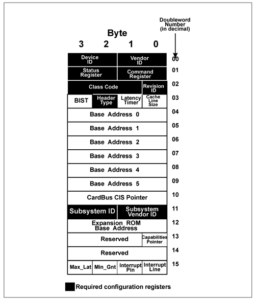
Header Type 0GeneralFigure 22-1 on page 771 illustrates the format of a function's Header region (for functions other than PCI-to-PCI bridges and CardBus bridges). The registers marked in black are always mandatory. Note that although many of the configuration registers in the figure are not marked mandatory, a register may be mandatory for a particular type of device. The subsequent sections define each register and any circumstances wherein it may be mandatory. Figure 22-1. Header Type 0
As noted earlier, this format is defined as Header Type 0. The registers within the Header are used to identify the device, to control its functionality and to sense its status in a generic manner. The usage of the device's remaining 48 dwords of PCI-compatible configuration space is intended for device-specific registers, but, with the advent of the 2.2 PCI spec, is also used as an overflow area for some new registers defined in the PCI spec (for more information, refer to "Capabilities Pointer Register" on page 779). Header Type 0 Registers Compatible With PCIThe Header Type 0 PCI configuration registers that are implemented and used identically in PCI and PCI Express are:
The sections that follow provide a description of each of these registers. Header Type 0 Registers Incompatible With PCIIn a non-bridge PCI Express function, the definitions of the following configuration registers in the function's PCI-compatible configuration space differ from the PCI spec's definition of the respective register definitions:
The sections that follow define the implementation/usage differences of these registers. For a full description of their implementation in a PCI function, refer to the MindShare book entitled PCI System Architecture, Fourth Edition (published by Addison-Wesley). For a full description of their implementation in a PCI-X function, refer to the MindShare book entitled PCI-X System Architecture, First Edition (published by Addison-Wesley). Registers Used to Identify Device's DriverThe OS uses some combination of the following mandatory registers to determine which driver to load for a device:
Vendor ID RegisterPCI-Compatible register. Always mandatory. This 16-bit register identifies the manufacturer of the function. The value hardwired in this read-only register is assigned by a central authority (the PCI SIG) that controls issuance of the numbers. The value FFFFh is reserved and must be returned by the Host/PCI bridge when an attempt is made to perform a configuration read from a configuration register in a non-existent function. In PCI or PCI-X, the read attempt results in a Master Abort, while in PCI Express it results in the return of UR (Unsupported Request) completion status. In either case, the bridge must return a Vendor ID of FFFFh. The error status returned is not considered to be an error, but the specification says that the bridge must nonetheless set its Received Master Abort bit in its configuration Status register. Device ID RegisterPCI-Compatible register. Always mandatory. This 16-bit value is assigned by the function manufacturer and identifies the type of function. In conjunction with the Vendor ID and possibly the Revision ID, the Device ID can be used to locate a function-specific (and perhaps revision-specific) driver for the function. Revision ID RegisterPCI-Compatible register. Always mandatory. This 8-bit value is assigned by the function manufacturer and identifies the revision number of the function. If the vendor has supplied a revision-specific driver, this is handy in ensuring that the correct driver is loaded by the OS. Class Code RegisterGeneralPCI-Compatible register. Always mandatory. The Class Code register is pictured in Figure 22-2 on page 775. It is a 24-bit, read-only register divided into three fields: base Class, Sub Class, and Programming Interface. It identifies the basic function of the function (e.g., a mass storage controller), a more specific function sub-class (e.g., IDE mass storage controller), and, in some cases, a register-specific programming interface (such as a specific flavor of the IDE register set).
Figure 22-2. Class Code Register
The currently-defined base Class codes are listed in Table 22-1 on page 775. Table 2 on page 1020 through Table 19 on page 1031 define the Subclasses within each base Class. For many Class/SubClass categories, the Programming Interface byte is hardwired to return zeros (in other words, it has no meaning). For some, such as VGA-compatible functions and IDE controllers, it does have meaning. This register is useful when the OS is attempting to locate a function that a Class driver can work with. As an example, assume that a particular device driver has been written to work with any display adapter that is 100% XGA register set-compatible. If the OS can locate a function with a Class of 03h (see Table 22-1 on page 775) and a Sub Class of 01h (see Table 5 on page 1022), the driver will work with that function. A Class driver is more flexible than a driver that has been written to work only with a specific function from a specific vendor. The Programming Interface ByteFor some functions (such as the XGA display adapter used as an example in the previous section) the combination of the Class Code and Sub Class Code is sufficient to fully-define its level of register set compatibility. The register set layout for some function types, however, can vary from one implementation to another. As an example, from a programming interface perspective there are a number of flavors of IDE mass storage controllers, so it's not sufficient to identify yourself as an IDE mass storage controller. The Programming Interface byte value (see Table 20 on page 1031) provides the final level of granularity that identifies the exact register set layout of the function. Detailed Class Code DescriptionA detailed description of the currently-defined Classes, SubClasses, and Programming Interface Byte values can be found in Appendix D.
Subsystem Vendor ID and Subsystem ID RegistersGeneralPCI-Compatible register. Mandatory. This register pair was added in revision 2.1 of the PCI spec and was optional. The 2.2 PCI spec and the PCI-X spec state that they are mandatory except for those functions that have a base Class of 06h (a Bridge) with a Sub Class of 00h-04h (refer to Table 8 on page 1023), or a base Class of 08h (Base System Peripherals) with a Sub Class of 00h-03h (see Table 10 on page 1026). This excludes bridges of the following types:
It also excludes the following generic system peripherals:
The Subsystem Vendor ID is obtained from the SIG, while the vendor supplies its own Subsystem ID (the full name of this register is really "Subsystem Device ID", but the "device" is silent). A value of zero in these registers indicates there isn't a Subsystem Vendor and Subsystem ID associated with the function. The Problem Solved by This Register PairA function may reside on a card or within an embedded device. Functions designed around the same PCI/PCI-X, or PCI Express core logic (produced by a third-party) may have the same Vendor and Device IDs (if the core logic vendor hardwired their own IDs into these registers). If this is the case, the OS would have a problem identifying the correct driver to load into memory for the function. These two mandatory registers (Subsystem Vendor ID and Subsystem ID) are used to uniquely identify the add-in card or subsystem that the function resides within. Using these two registers, the OS can distinguish the difference between cards or subsystems manufactured by different vendors but designed around the same third-party core logic. This permits the Plug-and-Play OS to locate the correct driver to load into memory. Must Contain Valid Data When First AccessedThese two registers must contain their assigned values before the system first accesses them. If software attempts to access them before they have been initialized, the device must issue:
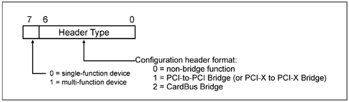
The values in these registers could be hardwired, loaded from a serial EEPROM, determined from hardware strapping pins, etc. Header Type RegisterPCI-Compatible register. Always mandatory. Figure 22-3 on page 778 illustrates the format of the Header Type register. Bits [6:0] of this one byte register define the format of dwords 4-through-15 of the function's configuration Header (see Figure 22-1 on page 771 and Figure 22-13 on page 803). In addition, bit seven defines the device as a single- (bit 7 = 0) or multifunction (bit 7 = 1) device. During configuration, the programmer determines if there are any other functions in this device that require configuration by testing the state of bit seven. Figure 22-3. Header Type Register Bit Assignment
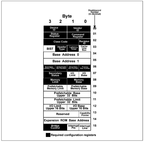
Figure 22-13. Header Type 1
Currently, the only Header formats defined other than that pictured in Figure 22-1 on page 771 (Header Type Zero) are:
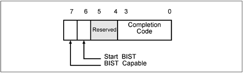
Future versions of the specification may define other formats. BIST RegisterPCI-Compatible register. Optional. This register may be implemented by both Requester and Completer functions. If a function implements a Built-In Self-Test (BIST), it must implement this register as illustrated in Figure 22-4 on page 778. Table 22-2 on page 779 describes each bit's function. If the function doesn't support a BIST, this register must return zeros when read. The function's BIST is invoked by setting bit six to one. The function resets bit six upon completion of the BIST. Configuration software must fail the function if it doesn't reset bit six within two seconds. At the conclusion of the BIST, the test result is indicated in the lower four bits of the register. A completion code of zero indicates successful completion. A non-zero value represents a function-specific error code. Figure 22-4. BIST Register Bit Assignment
The time limit of two seconds may not be sufficient time to test a very complex function or one with an extremely large buffer that needs to be tested. In that case, the remainder of the test could be completed in the initialization portion of the function's device driver when the OS loads it into memory and calls it.
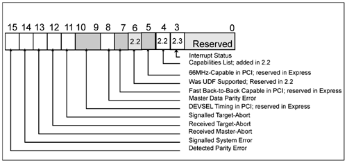
Capabilities Pointer RegisterPCI-Compatible register. Optional for a PCI function. Mandatory for a PCI-X or PCI Express function. Configuration Header Space Not Large EnoughThe 2.1 PCI spec defined the first 16 dwords of a function's PCI-compatible configuration space as its configuration Header space. It was originally intended that all of the function's PCI spec-defined configuration registers would reside within this region and that all of its function-specific configuration registers would reside within the lower 48 dwords of its PCI-compatible configuration space. Unfortunately, they ran out of space when defining new configuration registers in the 2.2 PCI spec. For this reason, the 2.2 and 2.3 PCI specs permit some spec-defined registers to be implemented in the lower 48 dwords of a function's PCI-compatible configuration space. Discovering That Capabilities ExistIf the Capabilities List bit in the Status register (see Figure 22-5 on page 780) is set to one, the function implements the Capabilities Pointer register in byte zero of dword 13 in its PCI-compatible configuration space (see Figure 22-1 on page 771). This implies that the pointer contains the dword-aligned start address of the Capabilities List within the function's lower 48 dwords of PCI-compatible configuration space. It is a rule that the two least-significant bits must be hardwired to zero and must be ignored (i.e., masked) by software when reading the register. The upper six bits represents the upper six bits of the 8-bit, dword-aligned start address of the new registers implemented in the lower 48 dwords of the function's PCI-compatible space. The two least-significant bits are assumed to be zero. Figure 22-5. Status Register
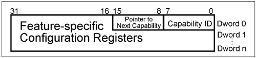
What the Capabilities List Looks LikeThe configuration location pointed to by the Capabilities Pointer register is the first entry in a linked series of one or more configuration register sets, each of which supports a feature. Each entry has the general format illustrated in Figure 22-6 on page 782. The first byte is referred to as the Capability ID (assigned by the PCI SIG) and identifies the feature associated with this register set (e.g., 2 = AGP), while the second byte either points to another feature's register set, or indicates that there are no additional register sets (with a pointer value of zero) associated with this function. In either case, the least-significant two bits must return zero. If a pointer to the next feature's register set is present in the second byte, it points to a dword within the function's lower 48 dwords of PCI-compatible configuration space (it can point either forward or backward in the function's configuration space). The respective feature's register set always immediately follows the first two bytes of the entry, and its length and format are defined by what type of feature it is. The Capabilities currently defined in the 2.3 PCI spec are those listed in Table 22-3 on page 781. Figure 22-6. General Format of a New Capabilities List Entry
CardBus CIS Pointer RegisterPCI-Compatible register. Optional. This optional register is implemented by functions that share silicon between a Cardbus device and a PCI or PCI Express function. This field points to the Card Information Structure (CIS) on the CardBus card. The register is read-only and indicates that the CIS can be accessed from the indicated offset within one of the following address spaces:
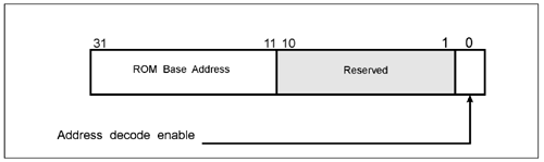
The format of the CardBus CIS Pointer register is defined in the revision 3.0 PC Card specification. A detailed description of the CIS can be found in the MindShare architecture series book entitled CardBus System Architecture (published by Addison-Wesley). Expansion ROM Base Address RegisterPCI-Compatible register. Required if a function incorporates a device ROM. Many PCI functions incorporate a device ROM (the spec refers to it as an expansion ROM) that contains a device driver for the function. The expansion ROM start memory address and size is specified in the Expansion ROM Base Address Register at configuration dword 12d in the configuration Header region. As described in the section entitled "Base Address Registers" on page 792, on power-up the system must be automatically configured so that each function's IO and memory decoders recognize mutually-exclusive address ranges. The configuration software must be able to detect how much memory space an expansion ROM requires. In addition, the system must have the capability of programming a ROM's address decoder in order to locate its ROM in a non-conflicting address range. When the start-up configuration program detects that a function has an Expansion ROM Base Address Register implemented (by writing all ones to it and reading it back), it must then check the first two locations in the ROM for an Expansion ROM signature to determine if a ROM is actually installed (i.e., there may be an empty ROM socket). If installed, the configuration program must shadow the ROM and execute its initialization code. This process is described in "Expansion ROMs" on page 871. The format of the expansion ROM Base Address Register is illustrated in Figure 22-7 on page 785:
Figure 22-7. Expansion ROM Base Address Register Bit Assignment
As an example, assume that the programmer writes FFFFFFFEh to the ROM's Base Address Register (bit 0, the Expansion ROM Enable bit, is cleared so as not to enable the ROM address decoder until a start memory address has been assigned). A subsequent read from the register in the example yields FFFE0000h. This indicates the following:
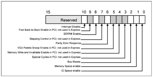
The PCI 2.3 spec recommends that the designer of the Expansion ROM Base Address Register should request a memory block slightly larger than that required by the current revision ROM to be installed. This permits the installation of subsequent ROM revisions that occupy more space without requiring a redesign of the logic associated with the function's Expansion ROM Base Address Register. The spec sets a limit of 16MB as the maximum expansion ROM size. The Memory Space bit in the Command register has precedence over the Expansion ROM Enable bit. The function's expansion ROM should respond to memory accesses only if both its Memory Space bit (in its Command register) and the Expansion ROM Enable bit (in its expansion ROM Base Address register) are both set to one. In order to minimize the number of address decoders that a function must implement, one address decoder can be shared between the Expansion ROM Base Address Register and one of the function's Memory Base Address Registers. The two Base Address Registers must be able to hold different values at the same time, but the address decoder will not decode ROM accesses unless the Expansion ROM Enable bit is set in the Expansion ROM Base Address Register. A more detailed description of expansion ROM detection, shadowing and usage can be found in "Expansion ROMs" on page 871. Command RegisterDiffers from the PCI spec. Mandatory. Refer to Figure 22-8 on page 785. Table 22-4 on page 786 provides a description of each bit in the Command register of a non-bridge function (i.e., one with a Type 0 Header format). Figure 22-8. Command Register
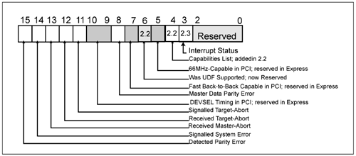
Status RegisterDiffers from the PCI spec. Mandatory. Table 22-5 on page 789 provides a description of each bit in the Status register (also refer to Figure 22-9 on page 788). The bit fields with the RW1C attribute have the following characteristics:
Figure 22-9. PCI Configuration Status Register
Cache Line Size RegisterDiffers from the PCI spec. Optional. This field is implemented by PCI Express devices as a read-write field for legacy compatibility purposes but has no impact on any PCI Express device functionality. Master Latency Timer RegisterDiffers from the PCI spec. Optional. This register does not apply to PCI Express and must be hardwired to 0. Interrupt Line RegisterDiffers from the PCI spec. Optional. Usage In a PCI FunctionRequired if a PCI function is capable of generating interrupt requests via an INTx# pin (i.e., INTA#, INTB#, INTC#, or INTD#). The PCI spec allows a function to generate interrupts either using an interrupt pin, or using MSI-capability (for more information, see "Message Signaled Interrupts" on page 331). The read/writable Interrupt Line register is used to identify which input on the interrupt controller the function's PCI interrupt request pin (as specified in its Interrupt Pin register; see "Interrupt Pin Register" on page 792) is routed to. For example, in a PC environment the values 00h-through-0Fh in this register correspond to the IRQ0-through-IRQ15 inputs on the interrupt controller. The value 255d (FFh) indicates "unknown" or "no connection." The values from 10h-through-FEh, inclusive, are reserved. Although it doesn't state this in the PCI spec, it is the author's opinion that RST# should initialize the Interrupt Line register to a value of FFh, thereby indicating that interrupt routing has not yet been assigned to the function. The OS or device driver can examine a device's Interrupt Line register to determine which system interrupt request line the device uses to issue requests for service (and, therefore, which entry in the interrupt table to "hook"). In a non-PC environment, the value written to this register is architecture-specific and therefore outside the scope of the specification. Usage In a PCI Express FunctionA PCI Express function may generate interrupts in the legacy PCI/PCI-X manner. As an example, when a PCI Express-to-PCI or PCI-X bridge detects the assertion or deassertion of one of its INTA#, INTB#, INTC#, or INTD# inputs on the legacy side of the bridge, it sends an INTx Assert or Deassert message upstream towards the Root Complex (specifically, to the interrupt controller within the Root Complex). As in PCI, the Interrupt Line register communicates interrupt line routing information. The register is read/write and must be implemented by any function that contains a valid non-zero value in its Interrupt Pin configuration register (described in the next section). The OS or device driver can examine a device's Interrupt Line register to determine which system interrupt request line the device uses to issue requests for service (and, therefore, which entry in the interrupt table to "hook"). In a non-PC environment, the value written to this register is architecture-specific and therefore outside the scope of the specification. Interrupt Pin RegisterDiffers from the PCI spec. Optional. Usage In a PCI FunctionRequired if a PCI function is capable of generating interrupt requests via an INTx# pin. The PCI spec allows a function to generate interrupts either using an interrupt pin, or using MSI-capability (for more information, see "Two Methods of Interrupt Delivery" on page 330). The read-only Interrupt Pin register defines which of the four PCI interrupt request pins, INTA#-through-INTD#, a PCI function is connected (i.e., bonded) to. The values 01h-through-04h correspond to PCI interrupt request pins INTA#-through-INTD#. A return value of zero indicates that the device doesn't generate interrupts. All other values (05h-FFh) are reserved. Usage In a PCI Express FunctionThis read-only register identifies the legacy INTx interrupt Message (INTA, INTB, INTC, or INTD) the function transmits upstream to generate an interrupt. The values 01h-through-04h correspond to legacy INTx interrupt Messages INTA-through-INTD. A return value of zero indicates that the device doesn't generate interrupts using the legacy method. All other values (05h-FFh) are reserved. Note that, although the function may not generate interrupts via the legacy method, it may generate them via the MSI method (see "Determining if a Function Uses INTx# Pins" on page 343 for more information). Base Address RegistersDiffer from the PCI spec. Required if a function implements memory and/or IO decoders. IntroductionVirtually all functions implement some memory, and/or a function-specific register set to control the function and sense its status. Some examples are:
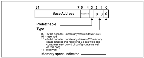
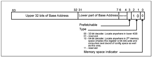
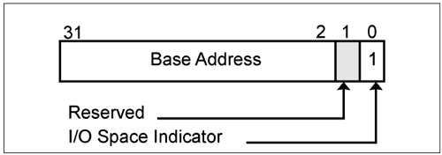
On power-up, the system must be automatically configured so that each function's IO and memory functions occupy mutually-exclusive address ranges. In order to accomplish this, the system must be able to detect how many memory and IO address ranges a function requires and the size of each. Obviously, the system must then be able to program the function's address decoders in order to assign non-conflicting address ranges to them. The Base Address Registers (BARs), located in dwords 4-through-9 of the function's configuration Header space (see Figure 22-1 on page 771), are used to implement a function's programmable memory and/or IO decoders. Each register is 32-bits wide (or 64-bits wide if it's a memory decoder and its associated memory block can be located above the 4GB address boundary). Figure 22-10 on page 796, Figure 22-11 on page 797, and Figure 22-12 on page 798 illustrate the three possible formats of a Base Address Register. Bit 0 is a read-only bit and indicates whether it's a memory or an IO decoder:
Figure 22-12. IO Base Address Register Bit Assignment
Decoders may be implemented in any of the Base Address Register positions. If more than one decoder is implemented, there may be holes. During configuration, the configuration software must therefore look at all six of the possible Base Address Register positions in a function's Header to determine which registers are actually implemented. IO Space UsageIn a PC environment, IO space is densely populated and will only become more so in the future. For this reason and because some processors are only capable of performing memory transactions, the following rules related to IO space usage are defined in the PCI Express spec:
Memory Base Address RegisterThis section provides a detailed description of the bit fields within a Memory BAR. The section entitled "Finding Block Size and Assigning Address Range" on page 799 describes how the register is probed to determine its existence, the size of the memory associated with the decoder, and the assignment of the base address to the decoder. Decoder Width FieldIn a Memory Base Address Register, bits [2:1] define whether the decoder is 32- or 64-bits wide:
Prefetchable Attribute BitBit three defines the block of memory as Prefetchable or not. A block of memory space may be marked as Prefetchable only if it can guarantee that:
In a nutshell, regular memory is prefetchable while memory-mapped IO (or any other badly-behaved memory region) is not. The configuration software can determine that a memory target is prefetchable or not by checking the Prefetchable bit in the memory target's Base Address Register (BAR). All memory BAR registers in PCI Express Endpoint functions with the Prefetchable bit set to one must be implemented as 64-bit memory BARs. Memory BARs that do not have the prefetchable bit set to one may be implemented as 32-bit BARs. As an example, the address decoder for a block of memory-mapped IO ports may hardwire the Prefetchable bit to zero, while the address decoder for well-behaved memory would hardwire it to one. For performance reasons, the spec urges that, wherever possible, memory-mapped IO ranges be marked as prefetchable memory. The configuration software checks this bit to determine a memory target's operational characteristics, assigns a memory range to its decoder (i.e., its Memory BAR), and then backtracks to all upstream bridges between the memory target and the processor and configures the bridges to treat the assigned memory range in the appropriate manner:
Base Address FieldThis field consists of bits [31:7] for a 32-bit memory decoder and bits [63:7] for a 64-bit memory decoder. It is used:
Programming of an example Memory Base Address Register is provided in "Finding Block Size and Assigning Address Range" on page 799. The minimum memory range requested by a BAR is 128 bytes. IO Base Address RegisterIntroductionThis section provides a detailed description of the bit fields within an IO Base Address Register. The section entitled "Finding Block Size and Assigning Address Range" on page 799 describes:
IO BAR DescriptionRefer to Figure 22-12 on page 798. Bit zero returns a one, indicating that this is an IO, rather than a memory, decoder. Bit one is reserved and must always return zero. Bits [31:2] comprises the Base Address field and is used to:
The PCI spec requires that a device that maps its control register set into IO space must not request more than 256 locations per IO Base Address Register. PC-Compatible IO DecoderThe upper 16-bits of the IO BAR may be hardwired to zero when a function is designed specifically for a PC-compatible, x86-based machine (because Intel x86 processors are incapable of generating IO addresses over 64KB). The function must still perform a full 32-bit decode of the IO address, however. Legacy IO DecodersLegacy PC-compatible devices such as VGA and IDE controllers frequently expect to be located within fixed legacy IO ranges. Such functions do not implement Base Address Registers. Instead, the configuration software identifies them as legacy functions via their respective Class Code and then enables their IO decoder(s) by setting the IO Space bit in its Command register to one. A legacy IO function may or may not own all of the byte locations within a dword of IO space:
Finding Block Size and Assigning Address RangeHow It WorksThe configuration program must probe each of a function's possible Base Address Registers to determine:
All of this information can be ascertained simply by writing all ones to the Base Address Register and then reading it back. A return value of zero indicates that the Base Address Register isn't implemented. Assuming that the value read is non-zero, scanning the returned value (assuming its non-zero) upwards starting at the least-significant bit of the Base Address field, the programmer determines the size of the required memory or the IO space by finding the least-significant bit that was successfully set to one. Bit zero of the register has a binary-weighted value of one, bit one a value of two, bit two a value of four, etc. The binary-weighted value of the least-significant bit set to one in the Base Address field indicates the required amount of space. This is also the first read/writable bit in the register and all of the bits above it are by definition read/writable. After discovering this information, the program then writes a base 32- or 64-bit memory address, or the base 32-bit IO address into the Base Address Register. A Memory ExampleAs an example, assume that FFFFFFFFh is written to the Base Address Register at configuration dword 04d and the value read back is FFF00000h. The fact that any bits could be changed to one indicates that the Base Address Register is implemented.
The programmer then writes a 32-bit base address into the register. However, only bits [31:20] are writable. The decoder accepts bits [31:20] and assumes that bits [19:0] of the assigned base address are zero. This means that the base address is divisible by 1MB, the size of the requested memory range. It is a characteristic of PCI, PCI-X, and PCI Express decoders that the assigned start address is always divisible by the size of requested range. As an example, it is possible to program the example memory address decoder for a 1MB block of memory to start on the one, two, or three meg boundary, but it is not possible to set its start address at the 1.5, 2.3, or 3.7 meg boundary. An IO ExampleAs a second example, assume that FFFFFFFFh is written to a function's Base Address Register at configuration dword address 05d and the value read back is FFFFFF01h. Bit 0 is a one, indicating that this is an IO address decoder. Scanning upwards starting at bit 2 (the least-significant bit of the Base Address field), bit 8 is the first bit that was successfully changed to one. The binary-weighted value of this bit is 256, indicating that this is an IO address decoder requesting 256 bytes of IO space. The programmer then writes a 32-bit base IO address into the register. However, only bits [31:8] are writable. The decoder accepts bits [31:8] and assumes that bits [7:0] of the assigned base address are zero. This means that the base address is divisible by 256, the size of the requested IO range. Smallest/Largest Decoder SizesSmallest/Largest Memory DecodersThe smallest memory address decoder is implemented as a Base Address Register that permits bits [31:7] to be written. Since the binary-weighted value of bit seven is 128, 128 bytes is the smallest memory block a memory decoder can be designed for. If a 32-bit memory BAR only permits bit 31 to be written, it is requesting 2GB of memory space. A 64-bit memory BAR could request more than 2GB of memory address space, resulting in none of the lower 32 bits in the BAR being writable. If this is the case, the programmer must also write all ones in the high dword of the BAR to determine how big a memory space the decoder requires. Smallest/Largest IO DecodersThe smallest IO decoder would be implemented as a Base Address Register that permitted bits [31:2] to be programmed. Since the binary-weighted value of bit two is 4, 4 bytes (a dword) is the smallest IO block an IO decoder can be designed for. The largest IO decoder would permit bits [31:8] to be written. The binary-weighted value of bit 8 is 256 and this is therefore the largest range that an IO decoder can request. Byte MergingA bridge may combine writes to a single dword within one entry in the posted-write buffer. This feature is recommended to improve performance and is only permitted in memory address ranges that are designated as prefetchable. As an example, assume that a Requester performs two memory writes:
These four locations reside within the same dword. The bridge could absorb the first two-byte write into a dword buffer entry and then absorb the second two byte write into the same dword buffer entry. When the bridge performs the memory write, it can complete it as a single access. It is a violation of the spec, however, for a bridge to combine separate byte writes to the same location into a single write. As an example, assume that a Requester performs four separate memory writes to the same dword: the first writes to location zero in the dword, the second to location zero again, the third to location one and the fourth to location two. When the bridge performs the posted writes, it has to perform a single memory write transaction to write the first byte to location zero. It then performs a second memory write transaction to write to locations zero (the second byte written to it by the Requester), one and two. Bridge Must Discard Unconsumed Prefetched DataA bridge that has prefetched memory read data for a Requester must discard any prefetched read data that the Requester doesn't actually end up reading. The following is an example scenario that demonstrates a problem that will result if a bridge doesn't discard prefetched data that wasn't consumed:
Min_Gnt/Max_Lat RegistersDiffers from the PCI spec. Optional. These registers do not apply to PCI Express. They must be read-only and hardwired to 0.  |

| [ Team LiB ] |
|