Message Signaled Interrupts
Message Signaled Interrupts (MSIs) are delivered to the Root Complex via memory write transactions. The MSI Capability register provides all the information that the device requires to signal MSIs. This register is set up by configuration software and includes the following information:
See "Description of 3DW And 4DW Memory Request Header Fields" on page 176 for a review of the Memory Write Transaction Header. Note that MSIs always have a data payload of 1DW.
The MSI Capability Register Set
A PCI Express function indicates its support for MSI via the MSI Capability registers. Each native PCI Express function must implement a single MSI register set within its own configuration space. Note that the PCI Express specification defines two register formats:
64-bit memory addressing format (Figure 9-2 on page 332) —
required by all native PCI Express devices and optionally implemented by Legacy endpoints.

32-bit memory addressing format (Figure 9-3 on page 332) —
optionally supported by Legacy endpoints.

The following sections describe each field within the MSI registers.
Capability ID
The Capability ID that identifies the MSI register set is 05h. This is a hardwired, read-only value.
Pointer To Next New Capability
The second byte of the register set either points to the next New Capability's register set or contains 00h if this is the end of the New Capabilities list. This is a hardwired, read-only value. If non-zero, it must be a dword-aligned value.
Message Control Register
Figure 9-4 on page 333 and Table 9-1 on page 333 illustrate the layout and usage of the Message Control register.
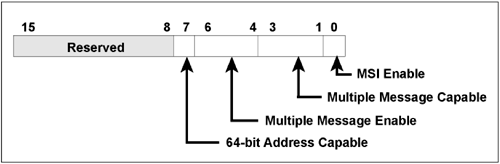
Table 9-1. Format and Usage of Message Control Register|
15:8 | Reserved | Read-Only. Always zero. | 7 | 64-bit Address Capable | Read-Only.
0 = Function does not implement the upper 32-bits of the Message Address register and is incapable of generating a 64-bit memory address. 1 = Function implements the upper 32-bits of the Message Address register and is capable of generating a 64-bit memory address.
| 6:4 | Multiple Message Enable | Read/Write. After system software reads the Multiple Message Capable field (see next row in this table) to determine how many messages are requested by the device, it programs a 3-bit value into this field indicating the actual number of messages allocated to the device. The number allocated can be equal to or less than the number actually requested. The state of this field after reset is 000b.
The field is encoded as follows: | Value | Number of Messages Requested | 000b | 1 | 001b | 2 | 010b | 4 | 011b | 8 | 100b | 16 | 101b | 32 | 110b | Reserved | 111b | Reserved | 3:1 | Multiple Message Capable | Read-Only. System software reads this field to determine how many messages the device would like allocated to it. The requested number of messages is a power of two, therefore a device that would like three messages must request that four messages be allocated to it. The field is encoded as follows: | Value | Number of Messages Requested | 000b | 1 | 001b | 2 | 010b | 4 | 011b | 8 | 100b | 16 | 101b | 32 | 110b | Reserved | 111b | Reserved | 0 | MSI Enable | Read/Write. State after reset is 0, indicating that the device's MSI capability is disabled.
0 = Function is disabled from using MSI. It must use INTX Messages to deliver interrupts (legacy endpoint or bridge). 1 = Function is enabled to use MSI to request service and is forbidden to use its interrupt pin.
|
Message Address Register
The lower two bits of the 32-bit Message Address register are hardwired to zero and cannot be changed. In other words, the address assigned by system software is always aligned on a dword address boundary.
The upper 32-bits of the Message Address register are required for native PCI Express devices and optional for legacy endpoints. This register is present if Bit 7 of the Message Control register is set. If present, it is a read/write register and it is used in conjunction with the Message Address register to assign a 32-bit or a 64-bit memory address to the device:
If the upper 32-bits of the Message Address register are set to a non-zero value by the system software, then a 64-bit message address has been assigned to the device using both the upper and lower halves of the register. If the upper 32-bits of the Message Address register are set to zero by the system software, then a 32-bit message address has been assigned to the device using both the upper and lower halves of the register.
Message Data Register
The system software assigns the device a base message data pattern by writing it into this 16-bit, read/write register. When the device must generate an interrupt request, it writes a 32-bit value to the memory address specified in the Message Address register. The data written has the following format:
The upper 16 bits are always set to zero. The lower 16 bits are supplied from the Message Data register. If more than one message has been assigned to the device, the device modifies the lower bits (the number of modifiable bits depends on how many messages have been assigned to the device by the configuration software) of the data from the Message Data register to form the appropriate message for the event it wishes to report to its driver. For an example, refer to the example cited in "Basics of Generating an MSI Interrupt Request" on page 338.
Basics of MSI Configuration
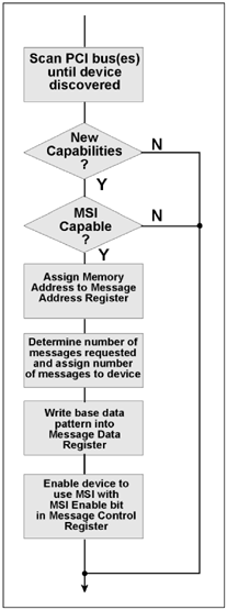
The following list specifies the steps taken by software to configure MSI interrupts for a PCI Express device. Refer to Figure 9-5 on page 337.
At startup time, the configuration software scans the PCI bus(es) (referred to as bus enumeration) and discovers devices (i.e., it performs configuration reads for valid Vendor IDs).When a PCI Express function is discovered, the configuration software reads the Capabilities List Pointer to obtain the location of the first Capability register within the chain of registers. The software then searches the capability register sets until it discovers the MSI Capability register set (Capability ID of 05h). Software assigns a dword-aligned memory address to the device's Message Address register. This is the destination address of the memory write used when delivering an interrupt request. Software checks the Multiple Message Capable field in the device's Message Control register to determine how many event-specific messages the device would like assigned to it. The software then allocates a number of messages equal to or less than what the device requested. At a minimum, one message will be allocated to the device. The software writes the base message data pattern into the device's Message Data register. Finally, the software sets the MSI Enable bit in the device's Message Control register, thereby enabling it to generate interrupts using MSI memory writes.
Basics of Generating an MSI Interrupt Request
When a PCI Express function generates an interrupt request to the processor it performs a memory write transaction. The associated data is platform specific and is always 1DW in size, and is written to a pre-defined memory address location. As described earlier, the configuration software is responsible for priming the function's MSI Address and Data registers with the appropriate memory address and the data to be written to that address when generating a request. It also primes a field in the Message Control register with the number of messages that have been allocated to the device.
Memory Write Transaction (MSI)
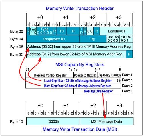
When the device must generate an interrupt request, it writes the Message Data register contents to the memory address specified in its Message Address register. Figure 9-6 on page 339 illustrates the contents of the Memory Write Transaction Header and Data field. Key points include:
Format field must be 11b, indicating a 4DW header with Data (native functions) and may be 10b for Legacy Endpoints. Header Attribute bits (No Snoop and Relaxed Ordering) must be zero. Length field must be 01h to indicate maximum data payload of 1DW. First BE field must be 0011b, indicating valid data in lower 16 bits. Last BE field must be 0000b, indicating a single DW transaction. Address fields within the header come directly from the address fields within the MSI Capability registers. Lower 16 bits of the Data payload come directly from the data field within the MSI Capability registers.
Multiple Messages
If the system software allocated more than one message to the device, it is permitted to modify the lower bits of the assigned Message Data value to send a different message for each device-specific event type that requires servicing by the device driver.
As an example, assume the following:
Four messages have been allocated to a device. A data value of 0500h has been assigned to the device's Message Data register. Memory address 0A000000h has been written into the device's Message Address register.
When any one of four different device-specific events occurs, the device generates a request by performing a dword write to memory address 0A000000h with a data value of 00000500h, 00000501h, 00000502h, or 00000503h. In other words, the device automatically appends the value 0000h to the upper part of its assigned message data value (to make a 32-bit value) and modifies the lower two bits of the value to indicate the specific message type.
Memory Synchronization When Interrupt Handler Entered
The Problem
Assume that a PCI Express device performs one or more memory write transactions to deliver data (application data) into main memory, followed by an MSI (which notifies software that new application data has been moved to memory). Also assume the following:
application data transactions have a Traffic Class of Zero (TC0) and will always flow through VC0 buffers. the MSI transaction uses TC1, and it flows through the VC1 buffers. These transactions traverse one or more switches on their way to the Root Complex and memory. VC arbitration is set up so that VC1 transactions have a much higher priority than VC0 transactions.
Flow Control and VC arbitration associated with the delivery of the data and the MSI may result in the MSI transaction being moved ahead of the application data transactions based on the goals of differentiated services. This is possible because there is no ordering relationship maintained between transactions that have different TC values and VC assignments. Consequently, the MSI may arrive at the Root Complex well ahead of the corresponding application data.
When the CPU is interrupted by the MSI, the currently-executing program is suspended and the processor executes the interrupt handler within the Requester's device driver. The driver may immediately read data from the target memory buffer in main memory. If some of the application data transactions that are still making their way upstream, the driver will fetch and process old data.
Solving the Problem
The problem can be solved in two ways:
Ensure that the TC numbers of the Memory Write data and the MSI are the same. The MSI must also have its relaxed ordering bit cleared. The driver can solve this problem by performing a dummy read (Memory Read Dword with all Byte Enables deasserted) from a location within its device before processing the data. The read must also have the same TC number as the Memory Write data. The read completion returned to the Root Complex will travel in the same VC as the Memory Write data, thereby ensuring that the write data will be pushed ahead of the read completion and into memory prior to the completion being received by the driver. Recall that the ordering rules require that all transactions with the same TC must be performed in order. The only exception is a transaction with the relaxed ordering bit set.
Interrupt Latency
The time from signaling an interrupt request until software services the device is referred to as its interrupt latency. As with the other interrupt request delivery mechanisms the MSI capability does not provide interrupt latency guarantees.
MSI Results In ECRC Error
Because MSIs are delivered as Memory Write transactions, and error associated with delivery of an MSI is treated the same as any other Memory Write error condition. See "ECRC Generation and Checking" on page 361 for treatment of ECRC errors.
Some Rules, Recommendations, etc.
It is the specification's intention that mutually-exclusive messages will be assigned to devices by the system software and that each message will be converted to an exclusive interrupt level upon delivery to the processor. More than one MSI capability register set per function is prohibited. A read from the Message Address register produces undefined results. Reserved registers and bits are read-only and always return zero when read. System software can modify Message Control register bits, but the device is prohibited from doing so. In other words, it's not permitted to modify the bits via the "back door." At a minimum, a single message will be assigned to each device. System software must not write to the upper half of the dword that contains the Message Data register. If the device writes the same message multiple times, only one of those messages is guaranteed to be serviced. If all of them must be serviced, the device must not generate the same message again until the driver services the earlier one. If a device has more than one message assigned, and it writes a series of different messages, it is guaranteed that all of them will be serviced.
 | 
