Function Power Management
PCI Express devices are required to support power management. Consequently, several registers and related bit fields must be implemented as discussed below.
The PM Capability Register Set
The PCI-PM specification defines the PM Capability register set that is located in PCI-compatible configuration space above the configuration header. The register is one in potentially many Capability registers that are linked together via pointers. The Capability ID of the PM register set is 01h. To determine the location of the PM registers software can perform the following checks. The registers described below must be implemented by PCI Express devices:
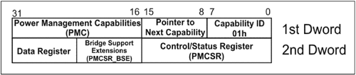
Software checks bit 4 (Capabilities List bit) of the function's Configuration Status register. A one indicates that the Capabilities Pointer register is implemented in the first byte of dword 13d of the function's configuration Header space. The programmer then reads the dword-aligned pointer from the Capabilities Pointer register and uses it to read the indicated dword from the function's configuration space. This is the first dword of the first New Capability register set. Refer to Figure 16-5 on page 586. If the first (i.e., least-significant) byte of the dword read contains Capability ID 01h, this identifies it as the PM register set used to control the function's power state. If the ID is something other than 01h, then this is the register set for a New Capability other than PM (e.g., PCI Express Capability registers). The byte immediately following the Capability ID byte is the Pointer to Next Capability field that specifies the start location (within the function's configuration space) of the register set for the next New Capability (if there are any additional New Capabilities). 00h indicates there isn't any, while a non-zero value is a valid pointer. As software traverses the linked-list of the function's New Capabilities, its PM register set will be located. A detailed description of the PM registers can be found in "Detailed Description of PCI-PM Registers" on page 596.
Device PM States
Each PCI Express function must support the full-on (D0) PM state and the full-off (D3) PM state. The D1 and D2 PM states are optional, as are the PM registers. The sections that follow provide a description of the possible PM states that may be supported by a PCI Express function.
D0 State—Full On
Mandatory
In this state, no power conservation is in effect and the device is fully-functional. All PCI Express functions must support the D0 state. There are two substates of the D0 PM state: D0 Uninitialized and D0 Active. No software-based power conservation is in effect in either of these two states. However, PCI Express defines Active State Power Management (ASPM) that is handled autonomously under hardware control to reduce link power consumption when the device is in this state. Table 16-6 on page 587 summarizes the PM policies while in the D0 state.
D0 Uninitialized
A function enters the D0 Uninitialized state in one of two ways:
As a result of the Fundamental Reset being dectected, or When commanded to transition from the D3hot to the D0 PM state by software.
In either case, the function exhibits all of the characteristics that it has after detecting Fundamental Reset. In other words, its registers are all returned to their default states (before the function was configured and enabled by software). The function exhibits the following characteristics:
It only responds to PCI Express configuration transactions. Its Command register enable bits are all returned to their default states. It cannot initiate transactions. It cannot act as the target of memory or IO transactions.
D0 Active
Once the function has been configured and enabled by software, it is in the D0 Active PM state and is fully functional.
Table 16-6. D0 Power Management Policies|
L0 | D0 uninitialized | PME context | < 10W | PCI Express config transactions. | None | L0
L0s (required) L1 (optional)[*] | D0 active | all | full | Any PCI Express transaction. | Any transaction, interrupt, or PME.[**] | L2/L3 | D0 active | N/A |
D1 State—Light Sleep
Optional.
This is a light sleep power conservation state. The function cannot:
initiate TLPs (except PME Message TLP, if enabled) act as the target of transactions other than PCI Express configuration transactions. The function's PM registers are implemented in its configuration space and software must be able to access these registers while the device is in the D1 state.
Other characteristics of the D1 state are:
Link automatically enters the L1 power conservation state when PM software places the function into the D1 state. The function may reactivate the link and send a PME message to notify PM software that the function has experienced an event that requires it be returned to full power (assuming that it supports the generation of PM events while in the D1 state and has been enabled to do so). The function may or may not lose its context in this state. If it does and the device supports PME, it must maintain its PME context (see "PM Event (PME) Context" on page 575) while in this state. The function must be returned to the D0 Active PM state in order to be fully-functional.
Table 16-7 lists the PM policies while in the D1 state.
Table 16-7. D1 Power Management Policies|
L1 | D1 | Device class-specific registers and PME context. |  D0 uninitialized D0 uninitialized
| PCI Express config transactions and transactions permitted by device class PM spec (typically none). This requires the device to transition from L1 back to L0, which is triggered by the upstream port detecting a configuration transaction targeting the device. | PME Messages. [**]
Transactions are typically not permitted (but device class spec may permit). This requires the device to transition from L1 back to L0, which is triggered by the internal PME. | L2-L3 | NA |
D2 State—Deep Sleep
Optional.
This power state provides more power conservation than the D1 PM state and less than the D3hot PM state. The function cannot:
initiate bus transactions act as the target of transactions other than PCI Express configuration transactions. The function's PM registers are implemented in its configuration space and software must be able to access these registers while the device is in the D2 state.
Other characteristics of the D2 state are:
The function transitions its link to the L1 state when PM software transitions function to the D2 state. The function may send a PME message to notify PM software that it needs to be returned to the active state to handle an event that has occurred (assuming that it supports the generation of PM events while in the D2 state and has been enabled to do so). The function may or may not lose its context in this state. If the function loses context and the device supports PME messages, it must maintain its PME context (see "PM Event (PME) Context" on page 575) while in this state. The function must be returned to the D0 Active PM state in order to be fully-functional.
Table 16-8 on page 590 illustrates the PM policies while in the D2 state.
Table 16-8. D2 Power Management Policies|
L1 | D2 | Device class-specific registers and PME context. | next lower supported PM state or D0 uninitialized. | PCI Express config transactions and transactions permitted by device class PM spec (typically none). This requires the device to transition from L1 back to L0, which is triggered by the upstream port detecting a configuration transaction targeting the device. | PME Messages.
Transactions are typically not permitted (but device class spec may permit). This requires the device to transition from L1 back to L0, which is triggered by the internal PME. | L2/L3 | N/A[**] |
D3—Full Off
Mandatory.
All functions must support the D3 PM state. This is the PM state in which power conservation is maximized. There are two ways that a function can be placed into the D3 PM state:
Removal of power (Vcc) from the device. This is referred to as the D3cold PM state. The function could transition into the D3cold state for one of two reasons: if the link it resides on is placed in the L2 or L3 state; or the system is unplugged. Power is still applied to the function and software commands the function to enter the D3 state. This is referred to as the D3hot PM state.
The following two sections describe the D3hot and D3cold PM states.
D3Hot State
Mandatory.
As mentioned in the previous section, a function is placed into the D3hot PM state under program control (by writing the appropriate value into the PowerState field of its PMCSR register).
The function cannot:
initiate bus transactions act as the target of transactions other than PCI Express configuration transactions. The function's PM registers are implemented in its configuration space and software must be able to access these registers while the device is in the D3hot state.
Other characteristics of the D3hot state are:
The function transitions its link to the L1 state when PM software transitions function to the D3hot state. The function may send a PME message to notify PM software of its need to be returned to the full active state (assuming that it supports the generation of PM events while in the D3hot state and has been enabled to do so). The function almost certainly loses its context in this state. If it does and the device supports the generation of PME messages while in the D3hot state, it must maintain its PME context (see "PM Event (PME) Context" on page 575) while in this state. The function must be returned to the D0 Active PM state in order to be fully-functional.
The function exits the D3hot state under two circumstances:
If Vcc is subsequently removed from the device, it transitions from D3hot to the D3cold PM state. Software can write to the PowerState field of the function's PMCSR register to change its PM state to D0uninitialized.
When programmed to exit D3hot and return to the D0 PM state, the function performs the equivalent of soft reset and returns to the D0 Uninitialized PM state (but Fundamental Reset is not required to be asserted). Table 16-9 on page 592 lists the PM policies while in the D3hot state.
Table 16-9. D3hot Power Management Policies|
L0 | | NA | L1 | D3hot | PME context. | next lower supported PM state or D0 uninitialized. | PCI Express config transactions
&
PME_Turn_Off broadcast message
(These can only occur after the link transitions back to its L0 state. | PME message[**]
PME_TO_ACK
message[***]
PM_Enter_L23 DLLP[***]
(These can occur only after the link returns to L0) | L2/L3 Ready | | L2/L3 Ready entered following the PME_Turn_Off handshake sequence, which prepares a device for power removal[***] | L2/L3 | | NA [*] |
D3Cold State
Mandatory.
Every PCI Express function enters the D3Cold PM state upon removal of power (Vcc) from the function. When power is restored, a Fundamental Reset must also be asserted. The function then transitions from the D3Cold state to the D0 Uninitialized state. A function capable of generating a PME from the D3Cold state must maintain its PME context while in this state and when transitioning to the D0 state. Since power has been removed from the function, the function must utilize some auxiliary power source to maintain the PME context. For more information on the auxiliary power source, refer to "Auxiliary Power" on page 645.
Table 16-10 on page 593 illustrates the PM policies while in the D3Cold state.
Table 16-10. D3cold Power Management Policies|
L0 | D3cold | | L1 | | L2 | PME context | AUX Power | Bus reset only | Signal Beacon
or
WAKE#[**] | L3 | None | None |
Function PM State Transitions
Figure 16-6 on page 594 illustrates the permissible PM state transitions for a PCI Express function. Table 16-11 on page 594 provides a description of each transition.
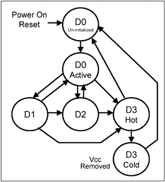
Table 16-12 on page 596 illustrates the delays involved in transitioning from one state to another from both a hardware and a software perspective.
Table 16-11. Description of Function State Transitions|
D0
Uninitialized | D0 Active | Occurs under program control when function has been completely configured and enabled by its driver. | D0 Active | D1 | Occurs when software writes to the PowerState field in the function's PMCSR register and sets the state to D1. | D2 | Occurs when software writes to the PowerState field in the function's PMCSR register and sets the state to D2. | D3hot | Occurs when software writes to the PowerState field in the function's PMCSR register and sets the state to D3hot. | D1 | D0 Active | Occurs when software writes to the PowerState field in the function's PMCSR register and sets the state to D0. | D2 | Occurs when software writes to the PowerState field in the function's PMCSR register and sets the state to D2. | D3hot | Occurs when software writes to the PowerState field in the function's PMCSR register and sets the state to D3hot. | D2 | D0 Active | Occurs when software writes to the PowerState field in the function's PMCSR register and sets the state to D0. | D3hot | Occurs when software writes to the PowerState field in the function's PMCSR register and sets the state to D3hot. | D3hot | D3cold | Occurs when the Power Control logic removes Power from the function. | D0
Uninitialized | Occurs when software writes to the PowerState field in the function's PMCSR register and sets the state to D0. | D3cold | D0
Uninitialized | Wake event causes power (Vcc) to be restored, Fundamental Reset also becomes active. This causes the function to return to the D0 Uninitialized state. If wake not supported, Fundamental Reset causes the transition to the D0 Uninitialized state. |
Table 16-12. Function State Transition Delays|
D0 | D1 | 0 | D0 or D1 | D2 | 200µs from new state setting to first access to function (including config accesses). | D0, D1, or D2 | D3hot | 10ms from new state setting to first access to function (including config accesses). | D1 | D0 | 0 | D2 | D0 | 200µs from new state setting to first access to function (including config accesses). | D3hot | D0 | 10ms from new state setting to first access to function (including config accesses). | D3cold | D0 |
Detailed Description of PCI-PM Registers
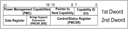
The PCI Bus PM Interface spec defines the PM registers (see Figure 16-7 on page 596) that are implemented in both PCI and PCI Express functions. These registers provide software with information regarding the function's PM capabilities and permit software to control the PM properties of the function. Since the PM registers are implemented in the PCI Express function's configuration space, software uses PCI configuration accesses to read and write the PM registers. The sections that follow provide a detailed description of these registers.
PM Capabilities (PMC) Register
Mandatory for function that implements PM.
This 16-bit read-only register is interrogated by software to determine the PM capabilities of the function. Figure 16-8 on page 597 illustrates the register and Table 16-13 on page 597 describes each bit field.
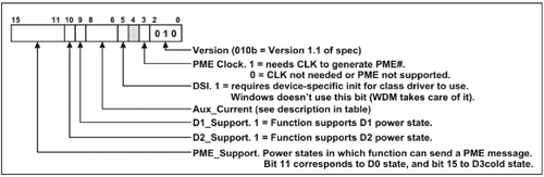
Table 16-13. The PMC Register Bit Assignments|
15:11 | PME_Support field. Indicates the PM states within which the function is capable of sending a PME message (Power Management Event). 0 in a bit indicates PME notification is not supported in the respective PM state. | Bit | Corresponds to PM State | 11 | D0 | 12 | D1 | 13 | D2 | 14 | D3hot | 15 | D3cold (function requires aux power for PME logic and Wake signaling via beacon or WAKE# pin) | Systems that support wake from D3cold must also support aux power. Similarly, components that support wake must use aux power to signal the wakeup.
Bits 31, 30, and 27 must be set to 1b for virtual PCI-PCI Bridges implemented within Root and Switch Ports. This is required for ports that forward PME Messages. | 10 | D2_Support bit. 1 = Function supports the D2 PM state. | 9 | D1_Support bit. 1 = Function supports the D1 PM state. | 8:6 | Aux_Current field. For a function that supports generation of the PME message from the D3cold state, this field reports the current demand made upon the 3.3Vaux power source (see "Auxiliary Power" on page 645) by the function's logic that retains the PME context information. This information is used by software to determine how many functions can simultaneously be enabled for PME generation (based on the total amount of current each draws from the system 3.3Vaux power source and the power sourcing capability of the power source).
If the function does not support PME notification from within the D3cold PM state, this field is not implemented and always returns zero when read. Alternatively, a new feature defined by PCI Express permits devices that do not support PMEs to report the amount of Aux current they draw when enabled by the Aux Power PM Enable bit within the Device Control register. If the function implements the Data register (see "Data Register" on page 603), this field is not implemented and always returns zero when read. The Data register then takes precedence over this field in reporting the 3.3Vaux current requirements for the function. If the function supports PME notification from the D3cold state and does not implement the Data register, then the Aux_Current field reports the 3.3Vaux current requirements for the function. It is encoded as follows:
| | | Bit
8 7 6 | Max Current Required | | | 1 1 1 | 375mA | | | 1 1 0 | 320mA | | | 1 0 1 | 270mA | | | 1 0 0 | 220mA | | | 0 1 1 | 160mA | | | 0 1 0 | 100mA | | | 0 0 1 | 55mA | | | 0 0 0 | 0mA | 5 | Device-Specific Initialization (DSI) bit. A one in this bit indicates that immediately after entry into the D0 Uninitialized state, the function requires additional configuration above and beyond setup of its PCI configuration Header registers before the Class driver can use the function. Microsoft OSs do not use this bit. Rather, the determination and initialization is made by the Class driver. | 4 | Reserved. | 3 | PME Clock bit. Does not apply to PCI Express. Must be hardwired to 0. | 2:0 | Version field. This field indicates the version of the PCI Bus PM Interface spec that the function complies with. | | | Bit 2 1 0 | Complies with Spec Version | | | 0 0 1 | 1.0 | | | 0 1 0 | 1.1 (required by PCI Express) |
PM Control/Status (PMCSR) Register
Mandatory for all PCI Express Devices. This register is used for the following purposes:
If the function implements PME capability, this register contains a PME Status bit that reflects whether or not a previously-enabled PME has occurred or not. If the function implements PME capability, this register contains a PME Enable bit that permits software to enable or disable the function's ability to assert the PME message or WAKE# signal. If the optional Data register is implemented (see "Data Register" on page 603), this register contains two fields that: The register's PowerState field can be used by software to determine the current PM state of the function and to place the function into a new PM state.
Figure 16-9 on page 600 and Table 16-14 on page 600 provide a description of the PMCSR bit fields. Note that PME is the abbreviation for Power Management Event.
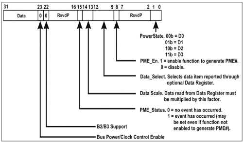
Table 16-14. PM Control/Status Register (PMCSR) Bit Assignments|
31:24 | all zeros | Read-only | See "Data Register" on page 603. | 23 | zero | Read-only | Not used in PCI Express | 22 | zero | Read-only | Not used in PCI Express | 21:16 | all zeros | Read-only | Reserved | 15 | See Description. | Read/Write. To Clear a one bit, write a one to it. | PME_Status bit. Optional.
Only implemented if the function supports PME notification, otherwise this bit is always zero.
If the function supports PME, this bit reflects whether the function has experienced a PME (even if the PME_En bit in this register has disabled the function's ability to send a PME message). If set to one, the function has experienced a PME. Software clears this bit by writing a one to it.
After reset, this bit is zero if the function doesn't support PME from D3cold. If the function supports PME from D3cold:
this bit is indeterminate at initial OS boot time. otherwise, it reflects whether the function has experienced a PME.
If the function supports PME from D3cold, the state of this bit must persist (is sticky) while the function remains in the D3cold state and during the transition from D3cold to the D0 Uninitialized state. This implies that the PME logic must use an aux power source to power this logic during these conditions (see "Auxiliary Power" on page 645). | 14:13 | Device-specific | Read-only | Data_Scale field. Optional.
If the function does not implement the Data register (see "Data Register" on page 603), this field is hardwired to return zeros.
If the Data register is implemented, the Data_Scale field is mandatory and must be implemented as a read-only field. The value read from this field represents the scaling factor that the value read from the Data register must be multiplied by. The value and interpretation of the Data_Scale field depends on the data item selected to be viewed through the Data register by the Data_Select field (see description in the next row of this table). | 12:9 | 0000b | Read/Write | Data_Select field. Optional.
If the function does not implement the Data register (see "Data Register" on page 603), this field is hardwired to return zeros.
If the Data register is implemented, the Data_Select field is mandatory and is implemented as a read/write field. The value placed in this register selects the data value to be viewed through the Data register. That value must then be multiplied by the value read from the Data_Scale field (see previous row in this table). | 8 | See Description. | PME_En bit. Optional.
1 = enable function's ability to send PME messages when an event occurs.
0 = disable.
If the function does not support the generation of PMEs from any power state, this bit is hardwired to always return zero when read.
After reset, this bit is zero if the function doesn't support PME from D3cold. If the function supports PME from D3cold:
this bit is indeterminate at initial OS boot time. otherwise, it enables or disables whether the function can send a PME message in case a PME occurs.
If the function supports PME from D3cold, the state of this bit must persist while the function remains in the D3cold state and during the transition from D3cold to the D0 Uninitialized state. This implies that the PME logic must use an aux power source to power this logic during these conditions. | 7:2 | all zeros | Read-only | Reserved | 1:0 | 00b | R/W | PowerState field. Mandatory.
Software uses this field to determine the current PM state of the function (by reading this field) or to place it into a new PM state (by writing to this field). If software selects a PM state that isn't supported by the function, the writes must complete normally, but the write data is discarded and no state change occurs. | 1 0 | PM State | 0 0 | D0 | 0 1 | D1 | 1 0 | D2 | 1 1 | D3hot |
Data Register
Optional, read-only.
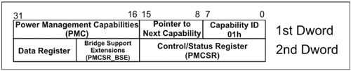
Refer to Figure 16-10 on page 605. The Data register is an optional, 8-bit, read-only register. If implemented, the Data register provides the programmer with the following information:
Power consumed in the selected PM state. This information is useful in power budgeting. Power dissipated in the selected PM state.This information is useful in managing the thermal environment. Other, device-specific information regarding the function's operational characteristics. Currently, the spec only defines power consumption and power dissipation information to be reported through this register.
If the Data register is implemented,
Determining Presence of the Data Register
Perform the following procedure to determine the presence of the Data register:
Write a value of 0000b into the Data_Select field of the PMCSR register. Read from either the Data register or the Data_Scale field of the PMCSR register. A non-zero value indicates that the Data register as well as the Data_Scale and Data_Select fields of the PMCSR registers are implemented. If a value of zero is read, go to step 3. If the current value of the Data_Select field is a value other than 1111b, go to step 4. If the current value of the Data_Select field is 1111b, all possible Data register values have been scanned and returned zero, indicating that neither the Data register nor the Data_Scale and Data_Select fields of the PMCSR registers are implemented. Increment the content of the Data_Select field and go to step 2.
Operation of the Data Register
The information returned is typically a static copy of the function's worst-case power consumption and power dissipation characteristics (obtained from the device's data sheet) in the various PM states. To use the Data register, the programmer uses the following sequence:
Write a value into the Data_Select field (see Table 16-15 on page 605) of the PMCSR register to select the data item to be viewed through the Data register. Read the data value from Data register. Multiply the value by the scaling factor read from the Data_Scale field of the PMCSR register (see "PM Control/Status (PMCSR) Register" on page 599).
Multi-Function Devices
In a multi-function PCI Express device, each function must supply its own power-oriented information and the power information related to their common logic must be reported through function zero's Data register (see Data Select Value = 8 in Table 16-15 on page 605).
Virtual PCI-to-PCI Bridge Power Data
The specification does not overtly state a requirement for PCI-to-PCI bridge functions that are part of a port within the Root Complex or Switch regarding data field use. However, to maintain PCI-PM compatibility bridges must report the power information they consume. In this same fashion software could read the virtual PPB Data registers at each port of a switch to determine the power consumed by the switch in each power state. Based on PCI-PM each PCI Express function would be responsible for reporting its own power-related data.
Table 16-15. Data Register Interpretation|
00h | Power consumed in D0 state | 00b = unknown
01b = multiply by 0.1
10b = multiply by 0.01
11b = multiply by 0.001 | Watts | 01h | Power consumed in D1 state | 02h | Power consumed in D2 state | 03h | Power consumed in D3 state | 04h | Power dissipated in D0 state | 05h | Power dissipated in D1 state | 06h | Power dissipated in D2 state | 07h | Power dissipated in D3 state | 08h | In a multi-function PCI device, function 0 indicates the power consumed by the logic that is common to all of the functions residing within this package. | 09h-0Fh. Spec actually shows this as decimal values 9-15. Author has chosen to represent in hex. | Reserved for future use of function 0 in a multi-function device. | Reserved | TBD | 08h-0Fh. Spec actually shows this as decimal values 8-15. Author has chosen to represent in hex. | Reserved (single function devices and other functions (greater than function 0) within a multi-function device |
 |

