| [ Team LiB ] |


|
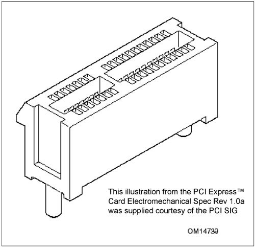
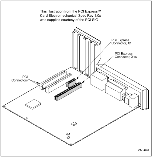
IntroductionOne goal of the PCI Express add-in card electromechanical spec was to encourage migration from the PCI architecture found in many desktop and mobile devices today by making the migration path straightforward and minimizing the required hardware changes. Towards this end, PCI Express add-in cards are defined to be very similar to the current PCI add-in card form factor, allowing them to readily coexist with PCI slots in system boards designed to the ATX or micro-ATX standard. PCI Express features like automatic polarity inversion and lane reversal also help reduce layout issues on system boards, so they can still be designed using the four-layer FR4 board construction commonly used today. As a result, much of an existing system board design can remain the same when it is modified to use the new architecture, and no changes are required for existing chassis designs. Add-in ConnectorThe PCI Express add-in card connector (see Figure 18-1 on page 687 and Figure 18-2 on page 688) is physically very similar to the legacy PCI connector, but uses a different pinout and does not supply -12V or 5V power. The physical dimensions of a card are the same as the PCI add-in cards and the same IO bracket is used. Table 18-1 on page 689 shows the pinout for a connector that supports PCI Express cards up to x16 (16 lanes wide). Several signals are referred to as auxiliary signals in the spec, and these are highlighted and described in more detail in the section that follows the table. Figure 18-1. PCI Express x1 connector
Figure 18-2. PCI Express Connectors on System Board
Note that cards with fewer lanes can be plugged into larger connectors that will accommodate more lanes. This is referred to as Up-plugging. The opposite case, installing a larger card into a smaller slot is called Down-plugging and, unlike PCI, is physically prevented in PCI Express by the connector keying.) Consequently, the connector described by the table will accommodate a card that is x1, x4, x8, or x16. This flexibility in the connector is highlighted by notes in the table that indicate each group of signals. For example, a x4 card plugged into this slot would only make use of pins 1 through 32, and so the note indicating the end of the x4 group of signals appears after pin 32. These segment indicators do not represent physical spaces or keys, however, because there is only one mechanical key on the connector, located between pins 11 and 12.
Auxiliary SignalsGeneralSeveral signals highlighted in Table 18-1 as auxiliary signals are described here in more detail. These signals are provided to assist with certain system level functions and are not required by the general PCI Express architecture, although some are required for add-in cards. For reference, these signals are summarized in Table 18-2.
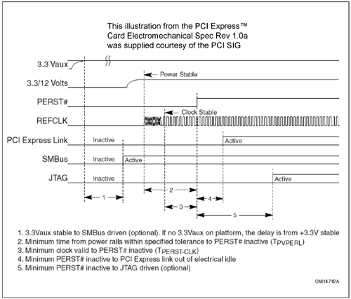
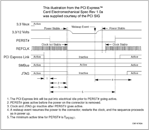
Reference ClockThis differential clock must be provided by the system board (although its use is optional for add-in cards). Its purpose is to allow both the transmitter and the receiver on a link to derive their internal clocks from the same source clock. While using the reference clock is not required, it does simplify the task of keeping the internal clocks between devices on either end of a link within the specified 600ppm of each other, since any two reference clocks are required to be within +/- 300ppm of their nominal 100MHz frequency. In addition, the base spec states that minimizing the L0s exit latency (i.e., the time required for the link to transition from the lower power L0s state back to L0) requires using a common reference clock. Finally, if Spread Spectrum Clocking (SSC) is to be used, it generally requires that both transmitters and receivers on a link must use the same reference clock. SSC allows the clock to be "down-modulated", or reduced in frequency, by as much as 0.5% and then brought back up to its nominal frequency at a rate not higher than 33KHz. Trying to modulate the clock frequency among devices that were not using the same reference clock would clearly be very difficult. PERST#This signal, similar in function to an inverted version of the POWERGOOD signal in a typical PC, is deasserted 100ms after the power supply is stable and within tolerance (see Figure 18-3 on page 695). PERST# is also aware of power management activity and so can also be used to give PCI Express devices some advance notice that power is about to be removed as a result of a power management operation (see Figure 18-4 on page 696). As long as PERST# remains asserted, all PCI Express functions are held in reset. Figure 18-3. PERST Timing During Power Up
Figure 18-4. PERST# Timing During Power Management States
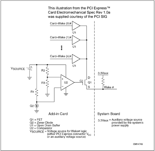
WAKE#This open-drain signal is driven by a PCI Express device that supports the wakeup function to request reactivation of the main power and reference clock. If an add-in card supports the wakeup process, it must implement this pin, and a system board must support the function if it connects to the WAKE# pin on the slot. There are actually two defined wakeup mechanisms, the side-band WAKE# signal and an in-band indicator called the Beacon. The Beacon is required for all components with the exception of certain form factors, of which the PCI Express add-in card is one example. Systems that support wakeup for these form factors are required to support the WAKE# signal for them although they are also encouraged to support the Beacon. Add-in cards that can generate a wakeup event are also required to support the Beacon operation. It is not clear why two mechanisms have been defined. One emphasis in PCI Express has been to reduce side-band signals, which would argue against adding a side-band wakeup signal. On the other hand, the use of the WAKE# signal may serve to reduce the latency involved in waking up the system enough to justify its use for add-in cards. If a slot supports WAKE#, the signal is routed to the platform power management controller, which might reside, for example, inside the Root Complex. The WAKE# signals from all the slots can be bussed together into a single input or they can each be used as separate inputs to the controller. WAKE# must have a system board pullup to a reference voltage that will be present when the main power rails are turned off, and the pullup must be a value that will allow it to pull WAKE# high in no more than 100ns. Note that Hot plug requires WAKE# to be isolated (between connectors) and driven inactive during hot-add or hot-remove operations. WAKE# functions in a way that is similar to PME# in a conventional PCI system, but it is not the same and must not be connected directly to the PME# signal. The spec also makes it clear that WAKE# must not directly cause an interrupt. As was true of the PME# signal in PCI, care must be taken to ensure that the generation of WAKE# in one device does not damage the WAKE# generation circuitry in another device. This could present a problem if one device has 3.3VAUX supplied while another does not, permitting the output buffers of the device without power to be reverse-biased by the assertion of WAKE# and possibly damaged. One solution to this problem is to add a circuit like the one shown in Figure 18-5. As would be expected, a card can only initiate a wakeup event if 3.3VAUX is supplied to it, since the other power rails may be turned off when the link is put into a sleep state. Figure 18-5. Example of WAKE# Circuit Protection
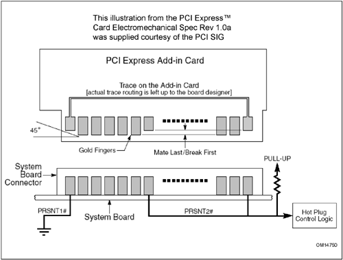
SMBusThis optional 2-wire bus provides a simple, inexpensive bus for system control and power management, reducing pin count and improving flexibility. One purpose for this bus is to reduce the number of control lines needed for the PCI Express bus, since it can be used to send SMBus messages between system devices. These messages can report manufacturer information, save state for a suspended event, report errors, accept control parameters, or supply status. The operation and requirements of the SMBus are described in detail in the System Management Bus Specification, Version 2.0. JTAGThis optional interface provides a Test Access Port (TAP) to facilitate testing of a card that implements it. The TAP pins operate at 3.3V, as do the other single-ended IO signals of the PCI Express connector. JTAG stands for Joint Test Action Group and is commonly used to refer to the IEEE Standard 1149.1, Test Access Port and Boundary Scan Architecture. PRSNT PinsRefer to Figure 18-6 on page 700. These pins are used by the system to indicate whether a card has been plugged into a connector. On the add-in card, the PRSNT1# pin is wired to the farthest available PRSNT2# pin on the connector. For example, a x4 card would wire pins 1A (PRSNT1#) and 31B (PRSNT2#) together on the card. On the system board the PRSNT1# pin on the slot is grounded, while all the PRSNT2# pins of the slot are bussed together and pulled high, so the system is able to detect that a card has been installed in the slot by observing that the PRSNT2# signal has been pulled low. Figure 18-6. Presence Detect
Detecting that a card has been added is useful in a system that implements either hot-plug or hot-swap mechanisms, since a slot could be left powered off when no card is detected. Upon insertion of a new card, the hardware could detect the change and begin the process of preparing the system to bring the new card online. When the new card goes active, the link will automatically detect that a device is present and begin the process of training the link. As an aside, the fact that an add-in card is required to connect PRSNT1# to the farthest possible PRSNT2# pin may mean that the spec designers considered using the presence detect pins to indicate information such as the link width on an add-in card. However, if the system board simply connects all the PRSNT2# pins together, this indication is not available. Visibility of the link width may have presented no real advantage anyway, since the link will automatically establish the usable link width during training. Electrical RequirementsPower Supply RequirementsTable 18-3 describes the power supplied to an add-in card. Note that the current provided by the +3.3V and +3.3VAUX supplies does not change as a function of the link width, while it does for the +12V supply, indicating that the +12V supply provides the power needed for add-in cards that have higher wattage requirements. Both the +3.3V and +12V power supplies are required for an add-in connector, while +3.3VAUX is optional. The current limits shown in the table for +3.3VAUX indicate that the higher allowance is only for devices that support wakeup. This resembles the power limits in PCI assigned for 3.3VAUX, in which the limit is based on whether a card is PME enabled, but there is an exception to the rule implied by this table in PCI Express. The configuration bit called Auxiliary Power PM Enable found in the Device Control Register (see "Device Control Register" on page 905), when set, indicates that a device has permission to use the full 375mA of auxiliary power regardless of whether it supports the wakeup function.
Power Dissipation LimitsThe power consumption limits for different link widths and card types are listed in Table 18-4. The table indicates, for example, that a x1 card cannot exceed 10W unless it is a high power device intended for server applications, in which case the maximum is 25W. At the high end, a x16 graphics card is allowed to consume up to 60W (increasing this value to 75W is under currently under consideration).
The difference between the types of cards is described in more detail in the electromechanical spec, but basically, the standard height cards intended for desktop applications are limited to half-length add-in cards with lower wattages, while cards intended for server applications must be from at least 7.0 inches long up to a full-length card and are allowed to use higher wattages. Low-profile cards are limited to half-length and lower wattages. Note that devices designated as high power are constrained to start up using the low power limits until they have been configured as high power devices. As a result, all x1 cards are initially limited to 10W, and cards intended for graphics applications are limited to 25W at initial power up until configured as a high power device, at which time they can use up to 60W (this may be increased to 75W in the future). See section "Slot Power Limit Control" on page 562 for more information on power configuration. Add-in Card InteroperabilityAs mentioned earlier, it is possible for a PCI Express add-in card to be plugged into a slot that was intended for a wider card. This is illustrated in Table 18-5, which also points out that all the slot widths must support the basic x1 card. There are basically three size-mismatch scenarios to consider:
 | ||||||||||||||||||||||||||||||||||||||||||||||||||||||||||||||||||||||||||||||||||||||||||||||||||||||||||||||||||||||||||||||||||||||||||||||||||||||||||||||||||||||||||||||||||||||||||||||||||||||||||||||||||||||||||||||||||||||||||||||||||||||||||||||||||||||||||||||||||||||||||||||||||||||||||||||||||||||||||||||||||||||||||||||||||||||||||||||||||||||||||||||||||||||||||||||||||||||||||||||||||||||||||||||||||||||||||||||||||||||||||||||||||||||||||||||||||||||||||||||||||||||||||||||||||||||
| [ Team LiB ] |
|