PCI Express Capability Register Set
Introduction
Refer to Figure 24-2 on page 897. Otherwise referred to as the PCI Express Capability Structure, implementation of the PCI Express Capability register set is mandatory for each function. It is implemented as part of the linked list of Capability register sets that reside in the lower 48 dwords of a function's PCI-compatible register area. It should be noted however, that some portions of this register set are optional.
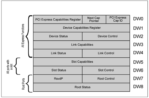
Register implementation requirements:
Every Express function must implement the registers that reside in dwords 0-through-4. The bridge associated with each Root Port must implement the registers that reside in dwords seven and eight. Each bridge associated with a Root Port or a downstream Switch Port that is connected to a slot (i.e., an add-in card slot) must implement the registers that reside in dwords five and six.
The sections that follow provide a detailed description of each of these registers.
Required Registers
General
The sections that follow describe each of the required registers within the PCI Express Capability register set. The following registers must be implemented by all Express functions:
PCI Express Capability ID Register Next Capability Pointer Register PCI Express Capabilities Register Device Capabilities Register Device Control Register Device Status Register Link Capabilities Register Link Control Register Link Status Register
PCI Express Capability ID Register
This read-only field must contain the value 10h, indicating this is the start of the PCI Express Capability register set.
Next Capability Pointer Register
This read-only field contains one of the following:
The dword-aligned, non-zero offset to the next capability register set in the lower 48 dwords of the function's PCI-compatible configuration space. 00h, if the PCI Express Capability register set is the final register set in the linked list of capability register sets in the function's PCI-compatible configuration space.
PCI Express Capabilities Register
Figure 24-3 on page 898 illustrates this register and Table 24-1 on page 899 provides a description of each bit field in this register.
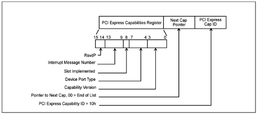
Table 24-1. PCI Express Capabilities Register|
3:0 | RO | Capability Version.
SIG-defined PCI Express capability structure version number (must be 1h). | 7:4 | RO | Device/Port Type.
Express logical device type:
0000b: PCI Express Endpoint.
Some OSs and/or processors may not support IO accesses (i.e., accesses using IO rather than memory addresses). This being the case, the designer of a native PCI Express function should avoid the use of IO BARs. However, the target system that a function is designed for may use the function as one of the boot devices (i.e., the boot input device (e.g., keyboard), output display device, or boot mass storage device) and may utilize a legacy device driver for the function at startup time. The legacy driver may assume that the function's device-specific register set resides in IO space. In this case, the function designer would supply an IO BAR to which the configuration software will assign an IO address range. When the OS boot has completed and the OS has loaded a native PCI Express driver for the function, however, the OS may deallocate all legacy IO address ranges previously assigned to the selected boot devices. From that point forward and for the duration of the power-up session, the native driver will utilize memory accesses to communicate with its associated function through the function's memory BARs.
0001b: Legacy PCI Express Endpoint.
A function that requires IO space assignment through BARs for run-time operations. Extended configuration space capabilities, if implemented on legacy PCI Express Endpoint devices, may be ignored by software.
0100b:
Root Port of PCI Express Root Complex.
0101b:
Switch upstream port[*].
0110b:
Switch downstream port[*].
0111b:
Express-to-PCI/PCI-X bridge[*].
1000b:
PCI/PCI-X to Express bridge[*]. All other encodings are reserved.
| 8 | HWInit | Slot Implemented.
When set, indicates that this Root Port or Switch downstream port is connected to an add-in card slot (rather than to an integrated component or being disabled). See "Chassis and Slot Number Assignment" on page 861 for more information. | 13:9 | RO | Interrupt Message Number.
If this function is allocated more than one MSI interrupt message value (see "Message Data Register" on page 335), this register contains the MSI Data value that is written to the MSI destination address when any status bit in either the Slot Status register (see "Slot Status Register" on page 925) or the Root Status register (see "Root Status Register" on page 928) of this function are set. If system software should alter the number of message data values assigned to the function, the function's hardware must update this field to reflect the change. |
Device Capabilities Register
Figure 24-4 on page 900 and Table 24-2 on page 901 provide a description of each bit field in this register. This register defines operational characteristics that are globally applicable to the device (and all functions that reside within it).
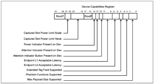
Table 24-2. Device Capabilities Register (read-only)|
2:0 | Max Payload Size Supported.
Max data payload size that the function supports for TLPs:
000b = 128 bytes max payload size 001b = 256 bytes max payload size 010b = 512 bytes max payload size 011b = 1KB max payload size 100b = 2KB max payload size 101b = 4KB max payload size 110b = Reserved 111b = Reserved
| 4:3 | Phantom Functions Supported.
Background:
Normally, each Express function (when acting as a Requester) is limited to no more than 32 outstanding requests currently awaiting completion (as indicated by the lower five bits of the transaction Tag; the upper three bits of the Tag must be zero). However, a function may require more than this. If the Extended Tag Field is supported (see bit 5 in this table) and if the Extended Tag Field Enable bit in the Device Control register is set (see "Device Control Register" on page 905), the max is increased to 256 and all eight bits of the Requester ID Tag field are used when a function within the device issues a request packet. If a function requires a greater limit than 256, it may do this via Phantom Functions.
Description:
When the device within which a function resides does not implement all eight functions, a non-zero value in this field indicates that this is so. Assuming all functions are not implemented and that the programmer has set the Phantom Function Enable bit in the Device Control register (see "Device Control Register" on page 905), a function may issue request packets using its own function number as well as one or more additional function numbers.
This field indicates the number of msbs of the function number portion of Requester ID that are logically combined with the Tag identifier.
00b.
The Phantom Function feature is not available within this device.
01b.
The msb of the function number in the Requestor ID is used for Phantom Functions. The device designer may implement functions 0-3. When issuing request packets, Functions 0, 1, 2, and 3 may also use function numbers 4, 5, 6, and 7, respectively, in the packet's Requester ID.
10b.
The two msbs of the function number in the Requestor ID are used for Phantom Functions. The device designer may implement functions 0 and 1. When issuing request packets, Function 0 may also use function numbers 2, 4, and 6 in the packet's Requester ID. Function 1 may also use function numbers 3, 5, and 7 in the packet's Requester ID.
11b.
All three bits of the function number in the Requestor ID are used for Phantom Functions. The device designer must only implement Function 0 (and it may use any function number in the packet's Requester ID).
| 5 | Extended Tag Field Supported.
Max supported size of the Tag field when this function acts as a Requester.
If 8-bit Tags are supported and will be used, this feature is enabled by setting the Extended Tag Field Enable bit in the Device Control register (see "Device Control Register" on page 905) to one. | 8:6 | Endpoint L0s Acceptable Latency.
Acceptable total latency that an Endpoint can withstand due to the transition from the L0s state to the L0 state (see "L0s Exit Latency Update" on page 625). This value is an indirect indication of the amount of the Endpoint's internal buffering. Power management software uses this value to compare against the L0s exit latencies reported by all components in the path between this Endpoint and its parent Root Port to determine whether ASPM L0s entry can be used with no loss of performance.
000b = Less than 64ns 001b = 64ns to less than 128ns 010b = 128ns to less than 256ns 011b = 256ns to less than 51 ns 100b = 512ns to less than 1µs 101b = 1µs to less than 2µs 110b = 2µs-4µs 111b = More than 4µs
| 11:9 | Endpoint L1 Acceptable Latency.
Acceptable latency that an Endpoint can withstand due to the transition from L1 state to the L0 state (see "L1 Exit Latency Update" on page 626). This value is an indirect indication of the amount of the Endpoint's internal buffering. Power management software uses this value to compare against the L1 Exit Latencies reported by all components in the path between this Endpoint and its parent Root Port to determine whether ASPM L1 entry can be used with no loss of performance.
000b = Less than 1µs 001b = 1µs to less than 2µs 010b = 2µs to less than 4µs 011b = 4µs to less than 8µs 100b = 8µs to less than 16µs 101b = 16µs to less than 32µs 110b = 32µs-64µs 111b = More than 64µs
| 12 | Attention Button Present.
When set to one, indicates an Attention Button is implemented on the card or module. Valid for the following PCI Express device Types:
| 13 | Attention Indicator Present.
When set to one, indicates an Attention Indicator is implemented on the card or module. Valid for the following PCI Express device Types:
| 14 | Power Indicator Present.
When set to one, indicates a Power Indicator is implemented on the card or module. Valid for the following PCI Express device Types:
| 25:18 | Captured Slot Power Limit Value (upstream ports only).
In combination with the Slot Power Limit Scale value (see the next row in this table), specifies the upper limit on power supplied by slot:
Power limit (in Watts) = Slot Power Limit value x Slot Power Limit Scale value
This value is either automatically set by the receipt of a Set Slot Power Limit Message received from the port on the downstream end of the link, or is hardwired to zero.
Refer to "Slot Power Limit Control" on page 562 for a detailed description. | 27:26 | Captured Slot Power Limit Scale (upstream ports only).
Specifies the scale used for the calculation of the Power Limit (see the previous row in this table):
00b = 1.0x 01b = 0.1x 10b = 0.01x 11b = 0.001x
This value is either automatically set by the receipt of a Set Slot Power Limit Message received from the port on the downstream end of the link, or is hardwired to zero. |
Device Control Register
Figure 24-5 on page 906 and Table 24-3 on page 906 provide a description of each bit field in this register.
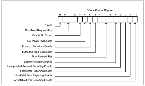
Table 24-3. Device Control Register (read/write)|
0 | Correctable Error Reporting Enable.
For a multifunction device, this bit controls error reporting for all functions. For a Root Port, the reporting of correctable errors occurs internally within the Root Complex. No external ERR_COR Message is generated.
Default value of this field is 0. | 1 | Non-Fatal Error Reporting Enable.
This bit controls the reporting of non-fatal errors. For a multifunction device, it controls error reporting for all functions. For a Root Port, the reporting of non-fatal errors occurs internally within the Root Complex. No external ERR_NONFATAL Message is generated.
Default value of this field is 0. | 2 | Fatal Error Reporting Enable.
This bit controls the reporting of fatal errors. For a multifunction device, it controls error reporting for all functions within the device. For a Root Port, the reporting of fatal errors occurs internally within the Root Complex. No external ERR_FATAL Message is generated.
Default value of this bit is 0. | 3 | Unsupported Request (UR) Reporting Enable.
When set to one, this bit enables the reporting of Unsupported Requests. For a multifunction device, it controls UR reporting for all functions. The reporting of error messages (ERR_COR, ERR_NONFATAL, ERR_FATAL) received by a Root Port is controlled exclusively by the Root Control register (see "Root Control Register" on page 926).
Default value of this bit is 0. | 4 | Enable Relaxed Ordering.
When set to one, the device is permitted to set the Relaxed Ordering bit (refer to "Relaxed Ordering" on page 319) in the Attributes field of requests it initiates that do not require strong write ordering.
Default value of this bit is 1, but it may be hardwired to 0 if a device never sets the Relaxed Ordering attribute in requests it initiates as a Requester. | 7:5 | Max Payload Size.
Sets the max TLP data payload size for the device. As a Receiver, the device must handle TLPs as large as the set value; as a Transmitter, the device must not generate TLPs exceeding the set value. Permissible values that can be programmed are indicated by the Max Payload Size Supported in the Device Capabilities register (see "Device Capabilities Register" on page 900).
000b = 128 byte max payload size 001b = 256 byte max payload size 010b = 512 byte max payload size 011b = 1024 byte max payload size 100b = 2048 byte max payload size 101b = 4096 byte max payload size 110b = Reserved 111b = Reserved
Default value of this field is 000b. | 8 | Extended Tag Field Enable.
When set to one, enables a device to use an 8-bit Tag field as a requester. If cleared to zero, the device is restricted to a 5-bit Tag field. Also refer to the description of the Phantom Functions Supported field in Table 24-2 on page 901.
The default value of this bit is 0. Devices that do not implement this capability hardwire this bit to 0. | 9 | Phantom Functions Enable.
See the description of the Phantom Functions Supported field in Table 24-2 on page 901.
Default value of this bit is 0. Devices that do not implement this capability hardwire this bit to 0. | 10 | Auxiliary (AUX) Power PM Enable.
When set to one, this bit enables a device to draw Aux power independent of PME Aux power. In a legacy OS environment, devices that require Aux power should continue to indicate PME Aux power requirements. Aux power is allocated as requested in the Aux Current field of the Power Management Capabilities register (PMC; see "Auxiliary Power" on page 645), independent of the PME Enable bit in the Power Management Control/Status register (PMCSR; see "PM Control/Status (PMCSR) Register" on page 599). For multifunction devices, a component is allowed to draw Aux power if at least one of the functions has this bit set.
Note:
Devices that consume Aux power must preserve the value in this field when Aux power is available. In such devices, this register value is not modified by hot, warm, or cold reset. Devices that do not implement this capability hardwire this bit to 0.
| 11 | Enable No Snoop.
Software sets this bit to one if the area of memory this Requester will access is not cached by the processor(s). When a request packet that targets system memory is received by the Root Complex (i.e., the memory that the processors cache from), the Root Complex does not have to delay the access to memory to perform a snoop transaction on the processor bus if the No Snoop attribute bit is set. This speeds up the memory access.
Note that setting this bit to one should not cause a function to unequivocally set the No Snoop attribute on every memory requests that it initiates. The function may only set the bit when it knows that the processor(s) are not caching from the area of memory being accessed. Default value of this bit is 1 and it may be hardwired to 0 if a device never sets the No Snoop attribute in Request transactions that it initiates.
| 14:12 | Max_Read_Request_Size.
Max read request size for the device when acting as the Requester. The device must not generate read requests with a size > this value.
000b = 128 byte max read request size 001b = 256 byte max read request size 010b = 512 byte max read request size 011b = 1KB max read request size 100b = 2KB max read request size 101b = 4KB max read request size 110b = Reserved 111b = Reserved
Devices that do not generate read requests larger than 128 bytes are permitted to implement this field as Read Only (RO) with a value of 000b.
Default value of this field is 010b. |
Device Status Register
Figure 24-6 on page 910 and Table 24-4 on page 910 provide a description of each bit field in this register.
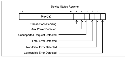
Table 24-4. Device Status Register|
0 | RW1C | Correctable Error Detected.
A one indicates that one or more correctable errors were detected since the last time this bit was cleared by software. Correctable errors are reflected by this bit regardless of whether error reporting is enabled or not in the Device Control register (see "Device Control Register" on page 905). In a multifunction device, each function indicates whether or not that function has detected any correctable errors using this bit.
For devices supporting Advanced Error Handling (see "Advanced Error Reporting Mechanisms" on page 382), errors are logged in this register regardless of the settings of the Correctable Error Mask register.
Default value of this bit is 0. | 1 | RW1C | Non-Fatal Error Detected.
A one indicates that one or more non-fatal errors were detected since the last time this bit was cleared by software. Non-fatal errors are reflected in this bit regardless of whether error reporting is enabled or not in the Device Control register (see "Device Control Register" on page 905). In a multifunction device, each function indicates whether or not that function has detected any non-fatal errors using this bit.
For devices supporting Advanced Error Handling, errors are logged in this register regardless of the settings of the Uncorrectable Error Mask register (note that the 1.0a spec says "Correctable Error Mask register", but the authors think this is incorrect).
Default value of this bit is 0. | 2 | RW1C | Fatal Error Detected.
A one indicates that one or more fatal errors were detected since the last time this bit was cleared by software. Fatal errors are reflected in this bit regardless of whether error reporting is enabled or not in the Device Control register (see "Device Control Register" on page 905). In a multifunction device, each function indicates whether or not that function has detected any fatal errors using this bit.
For devices supporting Advanced Error Handling (see "Advanced Error Reporting Capability" on page 930), errors are logged in this register regardless of the settings of the Uncorrectable Error Mask register (note that the 1.0a spec erroneously says "Correctable Error Mask register.")
Default value of this bit is 0. | 3 | RW1C | Unsupported Request (UR) Detected.
When set to one, indicates that the function received an Unsupported Request. Errors are reflected in this bit regardless of whether error reporting is enabled or not in the Device Control register (see "Device Control Register" on page 905). In a multifunction device, each function indicates whether or not that function has detected any UR errors using this bit.
Default value of this field is 0. | 4 | RO | Aux Power Detected.
Devices that require Aux power set this bit to one if Aux power is detected by the device. | 5 | RO | Transactions Pending.
When set to one, indicates that this function has issued non-posted request packets which have not yet been completed (either by the receipt of a corresponding Completion, or by the Completion Timeout mechanism). A function reports this bit cleared only when all outstanding non-posted requests have completed or have been terminated by the Completion Timeout mechanism.
|
Link Registers (Required)
There are three link-related registers:
The Link Capabilities Register. The Link Control Register. The Link Status Register.
Link Capabilities Register
Figure 24-7 on page 913 and Table 24-5 on page 913 provide a description of each bit field in this register.
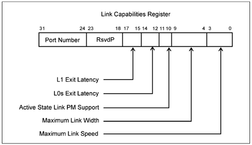
Table 24-5. Link Capabilities Register|
3:0 | RO | Maximum Link Speed.
| 9:4 | RO | Maximum Link Width.
| 11:10 | RO | Active State Power Management (ASPM) Support.
Indicates the level of ASPM supported on this Link.
Refer to "Link Active State Power Management" on page 608 for more information. | 14:12 | RO | L0s Exit Latency.
Indicates the L0s exit latency for the Link (i.e., the length of time this Port requires to complete a transition from L0s to L0).
000b = Less than 64ns 001b = 64ns to less than 128ns 010b = 128ns to less than 256ns 011b = 256ns to less than 512ns 100b = 512ns to less than 1µs 101b = 1µs to less than 2µs 110b = 2µs-4µs 111b = More than 4µs
Note:
Exit latencies may be influenced by a port's reference clock configuration (i.e., whether the port uses the reference clock supplied by the port at the remote end of the link or it provides it own local reference clock).
Refer to "ASPM Exit Latency" on page 624 for more information. | 17:15 | RO | L1 Exit Latency.
Indicates the L1 exit latency for the Link (i.e., the length of time this Port requires to complete a transition from L1 to L0).
000b = Less than 1µs 001b = 1µs to less than 2µs 010b = 2µs to less than 4µs 011b = 4µs to less than 8µs 100b = 8µs to less than 16µs 101b = 16µs to less than 32µs 110b = 32µs-64µs 111b = More than 64µs
Note:
Exit latencies may be influenced by a port's reference clock configuration (i.e., whether the port uses the reference clock supplied by the port at the remote end of the link or it provides it own local reference clock). Refer to "ASPM Exit Latency" on page 624 for more information. | 31:24 | HWInit | Port Number.
Indicates the Port number associated with this Link. The port number is assigned by the hardware designer. |
Link Control Register
Figure 24-8 on page 916 and Table 24-6 on page 916 provide a description of each bit field in this register.
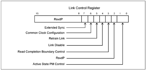
Table 24-6. Link Control Register|
1:0 | RW | Active State Power Management (ASPM) Control.
Controls the level of ASPM supported on the Link.
Default value of this field is 00b or 01b depending on form factor. At the time of writing, only the Electromechanical specified had been released. This specification makes no mention of the default state of the ASPM bits. | 3 | RO for Root and Switch Ports
RW for Endpoints | Read Completion Boundary (RCB).
Root Ports:
Hardwired. Indicates the RCB value for the Root Port. It is a hardwired, read-only value indicating the RCB support capabilities: - 0b = 64 byte - 1b = 128 byte
Endpoints:
Set by configuration software to indicate the RCB value of the Root Port upstream from the Endpoint. Devices that do not implement this feature must hardwire the field to 0b. - 0b = 64 byte - 1b = 128 byte
Switch Ports:
Reserved and hardwired to 0b.
| 4 | RW | Link Disable.
1 = disable the Link. Reserved on Endpoint devices and Switch upstream ports. The value written can be read back immediately, before the link has actually changed state.
Default value of this bit is 0b. | 5 | RW | Retrain Link.
1 = initiate Link retraining by changing the Physical Layer LTSSM to the Recovery state. Reads of this bit always return 0b. Reserved on Endpoint devices and Switch upstream ports. See "Link Errors" on page 379 for more information.
| 6 | RW | Common Clock Configuration.
1 indicates that this component and the component at the opposite end of this Link are using a common reference clock. 0 indicates that this component and the component at the opposite end of this Link are using separate reference clocks. A component factors this bit setting into its calculation of the L0s and L1 Exit Latencies (see Table 24-5 on page 913) that it reports in the Link Capabilities register. After changing this bit in a component on either end of a Link, software must trigger the Link to retrain by setting the Retrain Link bit to one in this register. Default value of this field is 0b.
See "ASPM Exit Latency" on page 624 for more information. | 7 | RW | Extended Sync.
When set to one, this bit forces the transmission of:
4096 FTS Ordered Sets during the L0s state followed by a single SKP ordered set prior to entering the L0 state, as well as the transmission of 1024 TS1 Ordered Sets in the L1 state prior to entering the Recovery state.
This mode gives external devices (e.g., logic analyzers) that may be monitoring Link activity time to achieve bit and symbol lock before the Link enters the L0 or Recovery state and resumes communication. Default value for this bit is 0b.
See "L0s State" on page 611 for more information. |
Link Status Register
Figure 24-9 on page 918 and Table 24-7 on page 919 provide a description of each bit field in this register.
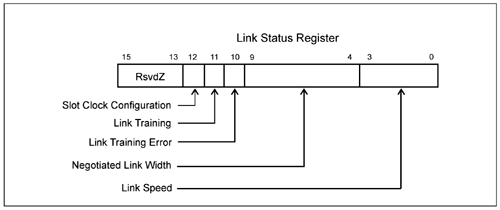
Table 24-7. Link Status Register|
3:0 | RO | Link Speed.
The negotiated Link speed.
All other encodings are reserved. | 9:4 | RO | Negotiated Link Width.
The negotiated Link width.
See "Negotiate Link Width[9:4]" on page 551 for more information. | 10 | RO | Training Error.
1 = indicates that a Link training error occurred. Reserved on Endpoint devices and Switch upstream ports. Cleared by hardware upon successful training of the Link to the L0 Link state.
See "Link Errors" on page 379 for more information. | 11 | RO | Link Training.
When set to one, indicates that Link training is in progress (Physical Layer LTSSM is in the Configuration or Recovery state) or that the Retrain Link bit was set to one but Link training has not yet begun.
See "Link Errors" on page 379 for more information. | 12 | HWInit | Slot Clock Configuration.
This bit indicates that the component uses the same physical reference clock that the platform provides on the connector. If the device uses an independent clock irrespective of the presence of a reference on the connector, this bit must be clear.
See "Config. Registers Used for ASPM Exit Latency Management and Reporting" on page 628 for more information. |
Slot Registers
Introduction
The slot-specific register set must be implemented for Root Port bridges and Switch downstream port bridges that are connected to add-in slot connectors. The registers are:
They are described in the sections that follow.
Slot Capabilities Register
Figure 24-10 on page 921 and Table 24-8 on page 921 provide a description of each bit field in this register.
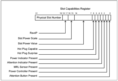
Table 24-8. Slot Capabilities Register (all fields are HWInit)|
0 | Attention Button Present.
1 = Attention Button is implemented on the chassis for this slot. | 1 | Power Controller Present.
1 = A Power Controller is implemented for this slot. | 2 | MRL (Manually-operated Retention Latch) Sensor Present.
1 = An MRL Sensor is implemented on the chassis for this slot. | 3 | Attention Indicator Present.
1 = An Attention Indicator is implemented on the chassis for this slot. | 4 | Power Indicator Present.
1 = A Power Indicator is implemented on the chassis for this slot. | 5 | Hot-Plug Surprise.
1 = A device installed in this slot may be removed from the system without any prior notification. | 6 | Hot-Plug Capable.
1 = This slot supports Hot-Plug operations. | 14:7 | Slot Power Limit Value.
In combination with the Slot Power Limit Scale value (see the next row in this table), specifies the max power (in Watts) available to the device installed in this slot.
Max power limit = Slot Power Limit Value x Slot Power Limit Scale value. This field must be implemented if the Slot Implemented bit is set to one in the PCI Express Capabilities Register (see "PCI Express Capabilities Register" on page 898). A write to this field causes the Port to send the Set Slot Power Limit Message upstream to the port at the other end of the Link. The default value prior to hardware/firmware initialization is 0000 0000b.
See "The Power Budget Capabilities Register Set" on page 564 for more information. | 16:15 | Slot Power Limit Scale.
See the description in the previous row of this table.
Possible values: - 00b = 1.0x - 01b = 0.1x - 10b = 0.01x - 11b = 0.001x
This field must be implemented if the Slot Implemented bit is set to one in the PCI Express Capabilities Register (see "PCI Express Capabilities Register" on page 898). A write to this field causes the Port to send the Set Slot Power Limit Message upstream to the port at the other end of the Link. The default value prior to hardware/firmware initialization is 00b.
| 31:19 | Physical Slot Number.
Indicates the physical slot number attached to this Port. Must be hardware initialized to a value that assigns a slot number that is globally unique within the chassis. Must be initialized to 0 for Ports connected to devices that are either integrated on the system board or integrated within the same silicon as the Switch downstream port or the Root Port.
See "Chassis and Slot Number Assignment" on page 861 for more information. |
Slot Control Register
Figure 24-11 on page 923 and Table 24-9 on page 924 provide a description of each bit field in this register.
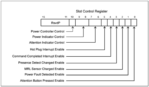
Table 24-9. Slot Control Register (all fields are RW)|
0 | Attention Button Pressed Enable.
When set to one, enables the generation of a Hot-Plug interrupt or a wakeup event when the attention button is pressed.
Default value of this field is 0. See "Attention Button" on page 667 for more information. | 1 | Power Fault Detected Enable.
When set to one, enables the generation of a Hot-Plug interrupt or a wakeup event on a power fault event. Default value of this field is 0. | 2 | MRL Sensor Changed Enable.
When set to one, enables the generation of a Hot-Plug interrupt or a wakeup event on an MRL sensor changed event. Default value of this field is 0.
See "Electromechanical Interlock (optional)" on page 667 for more information. | 3 | Presence Detect Changed Enable.
When set to one, enables the generation of a Hot-Plug interrupt or a wakeup event on a presence detect changed event.
Default value of this field is 0.
See "Slot Status and Events Management" on page 674 for more information. | 4 | Command Completed Interrupt Enable.
When set to one, enables the generation of a Hot-Plug interrupt when a command is completed by the Hot-Plug Controller.
Default value of this field is 0. | 5 | Hot-Plug Interrupt Enable.
When set to one, enables the generation of a Hot-Plug interrupt on enabled Hot-Plug events.
Default value of this field is 0. | 7:6 | Attention Indicator Control.
A read from this field returns the current state of the Attention Indicator, while a write sets the Attention Indicator to the state indicated below:
00b = Reserved 01b = On 10b = Blink 11b = Off
Writes to this field also cause the Port to send the respective Attention Indicator message. | 9:8 | Power Indicator Control.
A read from this field returns the current state of the Power Indicator, while a write sets the Power Indicator to the state indicated below:
00b = Reserved 01b = On 10b = Blink 11b = Off
Writes to this field also cause the Port to send the respective Power Indicator message. | 10 | Power Controller Control.
A read from this field returns the current state of the power applied to the slot, while a write sets the power state of the slot to the state indicated below:
0b = Power On 1b = Power Off
|
Slot Status Register
Figure 24-12 on page 925 and Table 24-10 on page 926 provide a description of each bit field in this register.
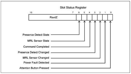
Table 24-10. Slot Status Register|
0 | RW1C | Attention Button Pressed.
1 = attention button pressed. | 1 | RW1C | Power Fault Detected.
1 = Power Controller detected a power fault at this slot. | 2 | RW1C | MRL Sensor Changed.
1 = MRL Sensor state change detected. | 3 | RW1C | Presence Detect Changed.
1 = Presence Detect change detected. | 4 | RW1C | Command Completed.
1 = Hot-Plug Controller completed a command. | 5 | RO | MRL Sensor State.
MRL sensor status (if MRL implemented).
0b = MRL Closed 1b = MRL Open
| 6 | RO | Presence Detect State.
When set to one, a card is present in the slot (as indicated either by an in-band mechanism or via the Presence Detect pins as defined in the PCI Express Card Electromechanical Specification).
This field must be implemented on all Switch downstream ports and on Root Ports that are attached to an add-in connector. It is hardwired to one if the port is not connected to an add-in slot connector. |
Root Port Registers
Introduction
All Root Ports must implement the Root Control and Root Status registers. The following two sections provide a detailed description of these two registers.
Root Control Register
Figure 24-13 on page 927 and Table 24-11 on page 927 provide a description of each bit field in this register.
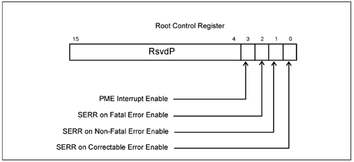
Table 24-11. Root Control Register (all fields are RW)|
0 | System Error on Correctable Error Enable.
When set to one, a System Error is generated if a correctable error (ERR_COR) is reported by any of the child (i.e., downstream) devices associated with this Root Port, or by the Root Port itself. The mechanism for signaling a System Error to the system is system-specific (e.g., in an x86-based system, a Non-Maskable Interrupt—NMI—could be generated to the processor).
Default value of this bit is 0.
See "Reporting Errors to the Host System" on page 392 for more information. | 1 | System Error on Non-Fatal Error Enable.
When set to one, a System Error is generated if a non-fatal error (ERR_NONFATAL) is reported by any of the child (i.e., downstream) devices associated with this Root Port, or by the Root Port itself. The mechanism for signaling a System Error to the system is system-specific (e.g., in an x86-based system, a Non-Maskable Interrupt—NMI—could be generated to the processor).
Default value of this bit is 0.
See "Reporting Errors to the Host System" on page 392 for more information. | 2 | System Error on Fatal Error Enable.
When set to one, a System Error is generated if a Fatal error (ERR_FATAL) is reported by any of the child (i.e., downstream) devices associated with this Root Port, or by the Root Port itself. The mechanism for signaling a System Error to the system is system-specific (e.g., in an x86-based system, a Non-Maskable Interrupt—NMI—could be generated to the processor).
Default value of this field is 0.
See "Reporting Errors to the Host System" on page 392 for more information. | 3 | PME Interrupt Enable.
When set to one, enables interrupt generation on receipt of a PME Message from a child (i.e., downstream) device (which sets the PME Status bit in the Root Status register—see "Root Status Register" on page 928—to one).
A PME interrupt is also generated when software sets this bit to one (assuming it was originally cleared to zero) when the PME Status bit in the Root Status register is set to one.
Default value of this field is 0.
See "The PME Sequence" on page 640 for more information. |
Root Status Register
Figure 24-14 on page 928 and Table 24-12 on page 929 provide a description of each bit field in this register.
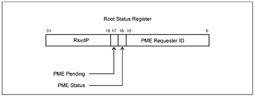
Table 24-12. Root Status Register|
15:0 | RO | PME Requestor ID.
Contains the Requester ID of the last child (i.e., downstream) device to issue a PME. | 16 | RW1C | PME Status.
When set to one, indicates that PME was asserted by the Requester indicated in the PME Requestor ID field. Subsequent PMEs remain pending until this bit is cleared by software by writing a 1 to it. | 17 | RO | PME Pending.
When set to one and the PME Status bit is set, indicates that another PME is pending. When the PME Status bit is cleared by software, the Root Port hardware indicates the delivery of the next PME by setting the PME Status bit again and updating the Requester ID field appropriately. The PME Pending bit is cleared by hardware when no more PMEs are pending. |
 |

