| [ Team LiB ] |


|
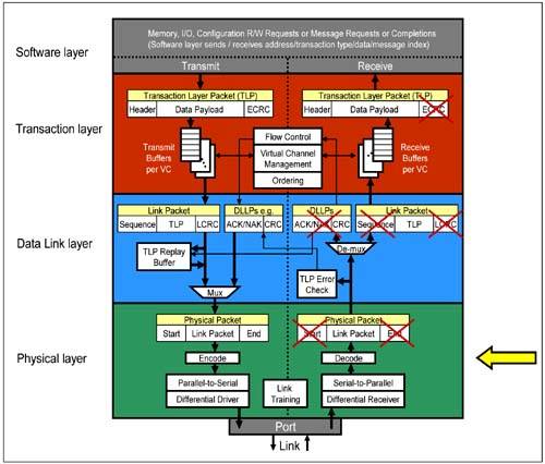
Physical Layer OverviewThe Physical Layer shown in Figure 11-1 on page 398 connects to the Link on one side and interfaces to the Data Link Layer on the other side. The Physical Layer processes outbound packets before transmission to the Link and processes inbound packets received from the Link. The two sections of the Physical Layer associated with transmission and reception of packets are referred to as the transmit logic and the receive logic throughout this chapter. Figure 11-1. Physical Layer
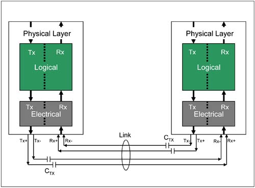
The transmit logic of the Physical Layer essentially processes packets arriving from the Data Link Layer, then converts them into a serial bit stream. The bit stream is clocked out at 2.5 Gbits/s/Lane onto the Link. The receive logic clocks in a serial bit stream arriving on the Lanes of the Link with a clock that is recovered from the incoming bit stream. The receive logic converts the serial bit steam into a parallel symbol stream, processes the incoming symbols, assembles packets and sends them to the Data Link Layer. In the future, data rates per Lane are expected to go to 5 Gbits/s, 10 Gbits/s and beyond. When this happens, an existing design can be adapted to the higher data rates by redesigning the Physical Layer while maximizing reuse of the Data Link Layer, Transaction Layer and Device Core/Software Layer. The Physical Layer may be designed as a standalone entity separate from the Data Link Layer and Transaction Layer. This allows a design to be migrated to higher data rates or even to an optical implementation if such a Physical Layer is supported in the future. Two sub-blocks make up the Physical Layer. These are the logical Physical Layer and the electrical Physical Layer as shown in Figure 11-2. This chapter describes the logical sub-block, and the next chapter describes the electrical sub-block. Both sub-blocks are split into transmit logic and receive logic (independent of each other) which allow dual simplex communication. Figure 11-2. Logical and Electrical Sub-Blocks of the Physical Layer
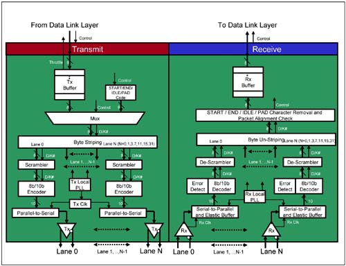
DisclaimerTo facilitate description of the Physical Layer functionality, an example implementation is described that is not necessarily the implementation assumed by the specification nor is a designer compelled to implement a Physical Layer in such a manner. A designer may implement the Physical Layer in any manner that is compliant with the functionality expected by the PCI Express specification. Transmit Logic OverviewFigure 11-3 on page 401 shows the elements that make up the transmit logic:
Figure 11-3. Physical Layer Details
TLPs and DLLPs from the Data Link layer are clocked into a Tx (transmit) Buffer. With the aid of a multiplexer, the Physical Layer frames the TLPs or DLLPs with Start and End characters. These characters are framing symbols which the receiver device uses to detect start and end of packet. The framed packet is sent to the Byte Striping logic which multiplexes the bytes of the packet onto the Lanes. One byte of the packet is transferred on one Lane, the next byte on the next Lane and so on for the available Lanes. The Scrambler uses an algorithm to pseudo-randomly scramble each byte of the packet. The Start and End framing bytes are not scrambled. Scrambling eliminates repetitive patterns in the bit stream. Repetitive patterns result in large amounts of energy concentrated in discrete frequencies which leads to significant EMI noise generation. Scrambling spreads energy over a frequency range, hence minimizing average EMI noise generated. The scrambled 8-bit characters (8b characters) are encoded into 10-bit symbols (10b symbols) by the 8b/10b Encoder logic. And yes, there is a 25% loss in transmission performance due to the expansion of each byte into a 10-bit character. A Character is defined as the 8-bit un-encoded byte of a packet. A Symbol is defined as the 10-bit encoded equivalent of the 8-bit character. The purpose of 8b/10b Encoding the packet characters is primarily to create sufficient 1-to-0 and 0-to-1 transition density in the bit stream so that the receiver can re-create a receive clock with the aid of a receiver Phase Lock Loop (PLL). Note that the clock used to clock the serial data bit stream out of the transmitter is not itself transmitted onto the wire. Rather, the receive clock is used to clock in an inbound packet. The 10b symbols are converted to a serial bit stream by the Parallel-to-Serial converter. This logic uses a 2.5 GHz clock to serially clock the packets out on each Lane. The serial bit stream is sent to the electrical sub-block which differentially transmits the packet onto each Lane of the Link. Receive Logic OverviewFigure 11-3 shows the elements that make up the receiver logic:
As the data bit stream is received, the receiver PLL is synchronized to the clock frequency with which the packet was clocked out of the remote transmitter device. The transitions in the incoming serial bit stream are used to re-synchronize the PPL circuitry and maintain bit and symbol lock while generating a clock recovered from the data bit stream. The serial-to-parallel converter is clocked by the recovered clock and outputs 10b symbols. The 10b symbols are clocked into the Elastic Buffer using the recovered clock associated with the receiver PLL. The Elastic Buffer is used for clock tolerance compensation; i.e. the Elastic Buffer is used to adjust for minor clock frequency variation between the recovered clock used to clock the incoming bit stream into the Elastic Buffer and the locally-generated clock associated that is used to clock data out of the Elastic Buffer. The 10b symbols are converted back to 8b characters by the 8b/10b Decoder. The Start and End characters that frame a packet are eliminated. The 8b/10b Decoder also looks for errors in the incoming 10b symbols. For example, error detection logic can check for invalid 10b symbols or detect a missing Start or End character. The De-Scrambler reproduces the de-scrambled packet stream from the incoming scrambled packet stream. The De-Scrambler implements the inverse of the algorithm implemented in the transmitter Scrambler. The bytes from each Lane are un-striped to form a serial byte stream that is loaded into the receive buffer to feed to the Data Link layer. Physical Layer Link Active State Power ManagementThe full-on power state of the Physical Layer and Link is called the L0 state. Devices support two lower power states, L0s (L0 suspend) and L1 Active that are actively and automatically managed by the Physical Layer. L1 Active power state is a lower power state than L0s and is optionally supported. The L0s power state is managed by the Physical Layer. The L1 Active power state is managed by a combination of Data Link Layer and Physical Layer. A Link can be placed in the L0s power state in one direction independent of the other direction while a Link in the L1 Active power state is in this state in both directions. Software enables support of the L0s and L1 Active power states via configuration registers. After reset, these registers are in a state that disables lower power state functionality. The Physical Layer automatically manages entering these lower power states upon detection of a period of inactivity on the Link. Once a device is in L0s or L1 Active and it intends to transmit packets, it can transition its Link power state back to L0. The exit latency from L1 Active is greater than the exit latency from L0s. Additional details on Link Active State Power Management are covered in "Link Training and Status State Machine (LTSSM)" on page 508 on Link Training and "Link Active State Power Management" on page 608. Link Training and InitializationThe Physical Layer is responsible for the Link Initialization and Training. The process is described in "Link Initialization and Training Overview" on page 500. |
| [ Team LiB ] |
|