Transmit Logic Details
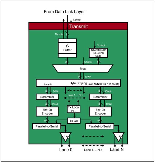
Figure 11-4 on page 406 shows the transmit logic of the Logical Physical Layer. This section describes packet processing from the time packets are received from the Data Link Layer until the packet is clocked out of the Physical Layer onto the Link.
Tx Buffer
The Tx Buffer receives TLPs and DLLPs from the Data Link Layer. Along with the packets, the Data Link Layer indicates the start and end of the packet using a 'Control' signal so that the Physical Layer can append Start and End framing characters to the packet. The Tx Buffer uses a 'throttle' signal to throttle the flow of packets from the Data Link Layer in case the Tx Buffer fills up.
Multiplexer (Mux) and Mux Control Logic
General
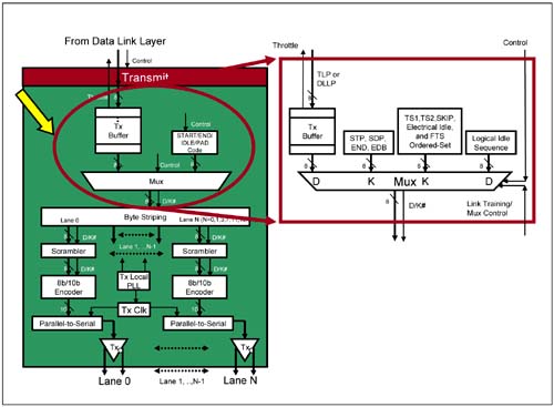
The Mux shown in Figure 11-5 on page 407 primarily gates packet characters from the Tx Buffer to the Byte Striping logic (only necessary if the link implements more than one data lane). However, under certain circumstances, the Mux may gate other inputs to the Byte Striping logic. Here is a summary of the four Mux inputs and when they are gated:
Transmit Data Buffer.
When the Data Link Layer supplies a packet to be transmitted, the Mux gates the packet's character stream through to the Byte Striping logic. Characters within the Tx Buffer are Data or 'D' characters. Hence the D/K# signal is driven High when Tx Buffer contents are gated. See "Definition of Characters and Symbols" on page 405.
Start and End characters.
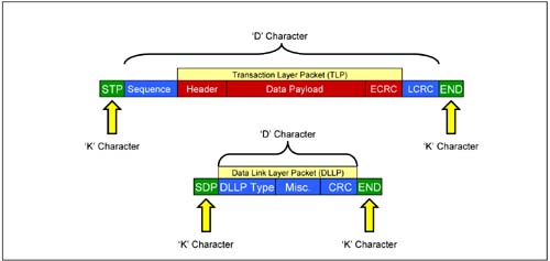
These Control characters are appended to the start and end of every TLP and DLLP as shown in Figure 11-6 on page 408. These framing characters allow a receiver to easily detect the start and end of a packet. There are two types of Start characters, one is the start TLP character (STP) and the other is the start DLLP character (SDP). There are two types of end characters, the End Good TLP or DLLP character (END), and the End Bad TLP character (EDB). See Table 11-5 on page 432 for a list of Control characters. A control signal from the Data Link Layer in combination with the packet type determine what type of framing character to gate. Start and End characters are Control or 'K' characters, hence the D/K# signal is driven low when the Start and End characters are gated out at the start and end of a packet, respectively.
Ordered-Sets.
Ordered-Sets are multiples of 4 character sequences that starts with a comma (COM) control character followed by other characters. They are transmitted during special events as described below: - During Link training, Training Sequence 1 and 2 (TS1 and TS2) Ordered-Sets are transmitted over the Link. Link training occurs after fundamental reset, hot reset, or after certain error conditions occur. Refer to "Ordered-Sets Used During Link Training and Initialization" on page 504 for detailed usage of TS1 and TS2 Ordered-Sets. - At periodic intervals, the Mux gates the SKIP Ordered-Set pattern through to the Byte Striping logic to facilitate clock tolerance compensation in the receiver circuit of the port at the other end of the Link. For a detailed description, refer to "Inserting Clock Compensation Zones" on page 436 and "Receiver Clock Compensation Logic" on page 442. - When a device wants to place its transmitter in the electrical Idle state, it must inform the remote receiver at the other end of the Link. The device gates an electrical Idle Ordered-Set to do so. - When a device wants to change the Link power state from L0s low power state to the L0 full-on power state, it transmits Fast Training Sequence (FTS) Ordered-Sets to the receiver. The receiver uses this Ordered-Set to re-synchronize its PLL to the transmitter clock.
Ordered-Sets begin with a K character and, depending on the type of set, may contain D or K characters. Hence, during transmission of an Ordered-Set, the D/K# signal is driven Low for a clock and then may be driven High or Low there after.
Logical Idle Sequence.
When there are no packets to transmit on the Link (referred to as Logical Idle Link), rather than leave the Link in a floating state or drive nothing, logical Idle characters are gated. Doing so guarantees signal transitions on the Link thus allowing the receiver's PLL to maintain clock synchronization with the transmit clock. In addition, the receiver is able to maintain bit and symbol lock. The logical Idle sequence consists of transmitting 00h characters. It therefore consists of D type characters, hence, the D/K# signal is high while the Mux is gating logical Idle sequences.
Definition of Characters and Symbols
Each character is 8-bits in size. They can be grouped into two categories, Control or 'K' characters, and Data or 'D' characters. From the standpoint of 8b/10b Encoding, D characters are encoded into a different 10-bit symbol than K characters of the same 8-bit value. Each 10-bit encoded character is referred to as a symbol.
Byte Striping (Optional)
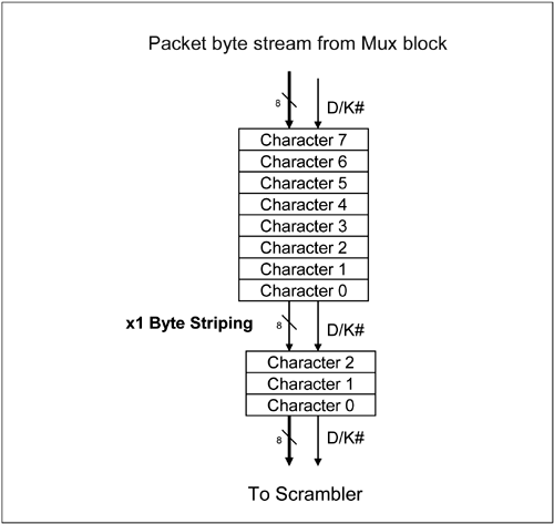
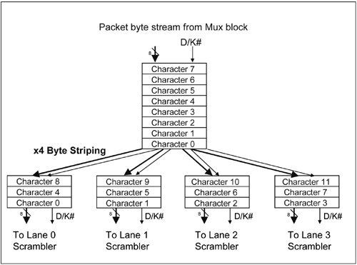
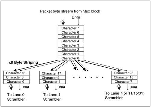
When a port implements more than one data Lane (i.e., more than one serial data path on the external Link), the packet data is striped across the 2, 4, 8, 12, 16, or 32 Lanes by the Byte Striping logic. Striping means that each consecutive outbound character in a character stream is multiplexed onto the consecutive Lanes. Examples of Byte Striping are illustrated in Figure 11-7 on page 409, Figure 11-8 on page 410, Figure 11-9 on page 411. The number of Lanes used is configured during the Link training process.
Disclaimer:
This example assumes that the Byte Striping logic is implemented before the Scrambler and 8b/10b Encoder. Every Lane implements a Scrambler and an 8b/10b Encoder. This permits a receiver Physical Layer to detect errors on any Lane independent of the other Lanes. For example, an error that may have occurred in the transmitter Scrambler or 8b/10b Encoder is detectable if a receiver detects an invalid 10b character on a given Lane. When an error is detected on a Lane and cannot be cleared, the Lane could be disabled and the Link re-trained and re-initialized with fewer Lanes. This error recovery feature is suggested and not required by specification.
On the other hand, to simplify and reduce the size of the Physical Layer logic, a designer may choose to place the Byte Striping logic after the Scrambler and 8b/10b Encoder but before the Parallel-to-Serial converter. This reduces the number of Scramblers and 8b/10b Encoders to one. If the receiver detects an error in the incoming bit stream however, it cannot isolate the error to a particular Lane.
Packet Format Rules
After passing through the Byte Striping logic, a TLP or DLLP character stream is striped across the Lanes. This section describes the rules used to byte stripe packets so that the packets are correctly striped across the Lanes of the Link.
General Packet Format Rules
The following are the general packet format rules:
The total packet length (including Start and End characters) of each packet must be a multiple of four characters. TLPs always start with the STP character. DLLPs always start with SDP and are 8 characters long (6 characters + SDP + END) All TLPs terminate with either an END or EDB character. DLLPs terminate with the END character. STP and SDP characters must be placed on Lane 0 when starting the transmission of a packet after the transmission of Logical Idles. If not starting a packet transmission from Logical Idle (i.e. back-to-back transmission of packets), then STP and SDP must start on a Lane number divisible by 4. Any violation of these rules may be reported as a Receiver Error to the Data Link Layer.
x1 Packet Format Example
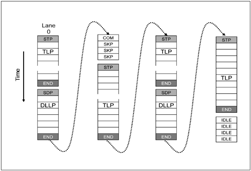
Figure 11-10 on page 413 illustrates the format of packets transmitted over a x1 Link (i.e., a Link with only one Lane operational). The illustration shows the following sequence of packets:
One TLP. One 8-byte DLLP. One clock compensation packet consisting of a SKIP Ordered-Set (i.e., a COM followed by three SKP characters). Two TLPs. One 8-byte DLLP. One TLP. A Flow Control Packet. Logical Idles transmitted because there are no more packets to transmit.
x4 Packet Format Rules
The following rules apply when a packet is transmitted over a x4 Link (i.e., a Link with four Lanes):
STP and SDP characters are always transmitted on Lane 0. END and EDB characters are always transmitted on Lane 3. When an Ordered-Set such as the SKIP Ordered-Set is transmitted (for clock compensation in the receiver), it must be sent on all four Lanes simultaneously. When Logical Idle sequences are transmitted, they must be transmitted on all Lanes. Any violation of these rules may be reported as a Receiver Error to the Data Link Layer.
x4 Packet Format Example
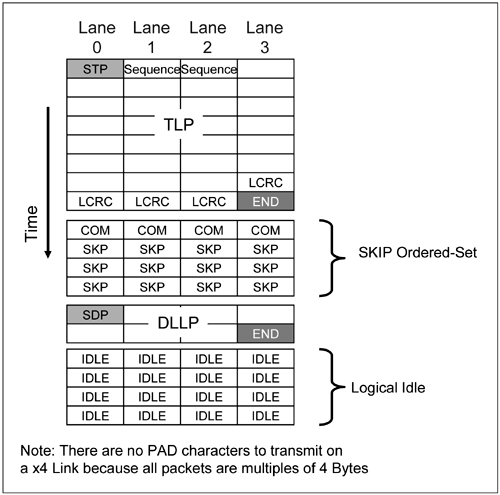
Figure 11-11 on page 414 illustrates the format of packets transmitted over a x4 Link (i.e., a Link with four data Lanes operational). The illustration shows the following sequence of packets:
One TLP. A SKIP Ordered-Set transmitted on all Lanes for periodic receiver clock compensation. A DLLP. Logical Idles on all Lanes because there are no more packets to transmit.
x8, x12, x16 or x32 Packet Format Rules
The following rules apply when a packet is transmitted over a x8, x12, x16, or x32 Link:
STP/SDP characters are always transmitted on Lane 0 when transmission starts after a period during which Logical Idles are transmitted. STP/SDP characters may only be transmitted on Lane numbers divisible by 4 when transmitting back-to-back packets. END/EDB characters are transmitted on Lane numbers divisible by 4 less 1. If a packet doesn't end on the last Lane and there are no more packet transmissions, PAD symbols are transmitted on the Lanes above the Lane on which the END/EDB character is transmitted. This keeps the Link aligned so that transmission of the Logical Idle sequence can start on all Lanes at the same time. When an Ordered-Set such as the SKIP Ordered-Set is transmitted (for clock compensation in the receiver), it must be sent on all four Lanes simultaneously. When Logical Idle sequences are transmitted, they must be transmitted on all Lanes. Any violation of these rules may be reported as a Receiver Error to the Data Link Layer.
x8 Packet Format Example
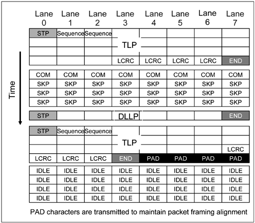
Figure 11-12 on page 415 illustrates the format of packets transmitted over a x8 Link (i.e., a Link with 8 Lanes operational). The illustration shows the following sequence of packets:
A TLP. A SKIP Ordered-Set transmitted on all Lanes for periodic receiver clock compensation. A DLLP. A TLP that ends on Lane 3. The remaining Lanes are filled with PADs so that the Link is aligned for the next transmission. Logical Idles on all Lanes because there are no more packets to transmit.
Scrambler
After byte striping, the outbound packets are transmitted across the Lanes. As shown in Figure 11-4 on page 406, each Lane in the Physical Layer design incorporates a Scrambler.
Purpose of Scrambling Outbound Transmission
The Scrambler eliminates generation of repetitive patterns on a transmitted data stream. As an example, when scrambled, a stream of 0s will result in a pseudo-random bit pattern.
Repetitive patterns result in large amount of energy concentrated in discrete frequencies which results in significant EMI noise generated. By scrambling the transmitted data, repetitive patterns—such as 10101010—are eliminated. As a result, no single frequency component of the signal is transmitted for significant periods of time. Thus the radiated EMI energy of a transmission is spread over a range in the frequency spectrum. This technique referred to as 'spread spectrum' effectively 'whitens' the frequency content of a signal and reduces the radiated power at any particular frequency.
On a bare systemboard with the wires of the Link un-shielded and high frequency transmission of 2.5 Gbits/s, EMI noise generation is significant. Scrambling makes the radiated power from the Link effectively look like white noise. This helps meet FCC requirements.
Also, on a multi-Lane Link with wires routed in close proximity, a scrambled transmission on one Lane generates white noise which does not interfere or correlate with another Lane's data transmission. This 'spatial frequency de-correlation' or reduction of crosstalk noise assists the receiver on each Lane to distinguish the desired signal from the background white noise.
Scrambler Algorithm
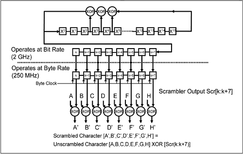
The Scrambler in Figure 11-13 on page 418 is implemented with a 16-bit Linear Feedback Shift Registers (LFSR) that implements the polynomial:
G(x) = X16 + X5 + X4+ X3 +1
The LFSR is clocked at the bit transfer rate. The LFSR output is serially clocked into an 8-bit register that is XORed with the 8-bit characters to form the scrambled data.
Implementation Note:
The LFSR bit rate clock is 8 times the frequency (2GHz) of the byte clock (250MHz) that feeds the Scrambler output.
Some Scrambler implementation rules:
On a multi-Lane Link implementation, Scramblers associated with each Lane must operate in concert, maintaining the same simultaneous value in each LFSR. Scrambling is applied to 'D' characters associated with TLP and DLLPs, including the Logical Idle (00h) sequence. 'D' characters within the TS1 and TS2 Ordered-Set are not scrambled. 'K' characters and characters within Ordered-Sets—such as TS1, TS2, SKIP, FTS and Electrical Idle Ordered-Sets—are not scrambled. These characters bypass the scrambler logic. Compliance Pattern related characters are not scrambled. When a COM character exits the Scrambler, (COM does not get scrambled) it initializes the LFSR. The initialized value of the 16-bit LFSR is FFFFh. Similarly on the receiver side, when a COM character enters the De-Scrambler, it is initialized. With one exception, the LFSR serially advances eight times for every character (D or K character) transmission. The LFSR does NOT advance on SKP characters associated with the SKIP Ordered-Set. The reason the LFSR is not advanced for SKPs is because a receiver of inbound packets may add or delete SKP symbols to perform clock tolerance compensation. Changing the number of characters in the receiver from the number of characters transmitted will cause the value in the receiver LFSR to lose synchronization with the transmitter LFSR value. For a detailed description, refer to "Inserting Clock Compensation Zones" on page 436 and "Receiver Clock Compensation Logic" on page 442. By default, Scrambling is always enabled. Although the specification does allow the Scrambler to be disabled for test and debug purposes, it does not provide a standard software or configuration register-related method to disable the Scrambler.
Disabling Scrambling
As stated in the previous section, the Scrambler can be disabled to help facilitate test and debug. Software or test equipment may tell a device to disable scrambling. However, the specification does not indicate the mechanism by which a device's Physical Layer is instructed to disable scrambling.
Scrambling is disabled in the Configuration State of Link Training described on the page 519. The device receiving the software request to disable scrambling will do so during the Link Training Configuration State, and transmits at least two TS1/TS2 Ordered-Sets with the disable scrambling bit set on all its configured Lanes to the remote device it is connected to. The remote receiver device disables its Scrambler/De-Scrambler. It is required that the Port that is sending the Disable Scrambling request will also disable scrambling.
8b/10b Encoding
General
Each Lane of a device's transmitter implements an 8-bit to 10-bit Encoder that encodes 8-bit data or control characters into 10-bit symbols. The coding scheme was invented by IBM in 1982 and is documented in the ANSI X3.230-1994 document, clause 11 (and also IEEE 802.3z, 36.2.4) and US Patent Number 4,486,739 entitled "Byte Oriented DC Balanced 8b/10b Partitioned Block Transmission Code". 8b/10b coding is now widely used in architectures such as Gigabit Ethernet, Fibre Channel, ServerNet, FICON, IEEE1394b, InfiniBand, etc.
Purpose of Encoding a Character Stream
The primary purpose of this scheme is to embed a clock into the serial bit stream transmitted on all Lanes. No clock is therefore transmitted along with the serial data bit stream. This eliminates the need for a high frequency 2.5GHz clock signal on the Link which would generate significant EMI noise and would be a challenge to route on a standard FR4 board. Link wire routing between two ports is much easier given that there is no clock to route, removing the need to match clock length to Lane signal trace lengths. Two devices are connected by simply wiring their Lanes together.
Below is a summary of the advantages of 8b/10b encoding scheme:
Embedded Clock.
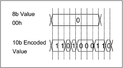
Creates sufficient 0-to-1 and 1-to-0 transition density (i.e., signal changes) to facilitate re-creation of the receive clock on the receiver end using a PLL (by guaranteeing a limited run length of consecutive ones or zeros). The recovered receive clock is used to clock inbound 10-bit symbols into an elastic buffer. Figure 11-14 on page 420 illustrates the example case wherein 00h is converted to 1101000110b, where an 8-bit character with no transitions has 5 transitions when converted to a 10b symbol. These transitions keep the receiver PLL synchronized to the transmit circuit clock: - Limited 'run length' means that the encoding scheme ensures the signal line will not remain in a high or low state for an extended period of time. The run length does not exceed five consecutive 1s or 0s. - 1s and 0s are clocked out on the rising-edge of the transmit clock. At the receiver, a PLL can recreate the clock by sync'ing to the leading edges of 1s and 0s. - Limited run length ensures minimum frequency drift in the receiver's PLL relative to the local clock in the transmit circuit.
DC Balance.
Keeps the number of 1s and 0s transmitted as close to equal as possible, thus maintaining DC balance on the transmitted bit stream to an average of half the signal threshold voltage. This is very important in capacitive- and transformer-coupled circuits. - Maintains a balance between the number of 1s and 0s on the signal line, thereby ensuring that the received signal is free of any DC component. This reduces the possibility of inter-bit interference. Inter-bit interference results from the inability of a signal to switch properly from one logic level to the other because the Lane coupling capacitor or intrinsic wire capacitance is over-charged.
Encoding of Special Control Characters.
Permits the encoding of special control ('K') characters such as the Start and End framing characters at the start and end of TLPs and DLLPs.
Error Detection.
A secondary benefit of the encoding scheme is that it facilitates the detection of most transmission errors. A receiver can check for 'running disparity' errors, or the reception of invalid symbols. Via the running disparity mechanism (see "Disparity" on page 423), the data bit stream transmitted maintains a balance of 1s and 0s. The receiver checks the difference between the total number of 1s and 0s transmitted since link initialization and ensures that it is as close to zero as possible. If it isn't, a disparity error is detected and reported, implying that a transmission error occurred.
The disadvantage of 8b/10b encoding scheme is that, due to the expansion of each 8-bit character into a 10-bit symbol prior to transmission, the actual transmission performance is degraded by 25% or said another way, the transmission overhead is increased by 25% (everything good has a price tag).
Properties of 10-bit (10b) Symbols
For 10-bit symbol transmissions, the average number of 1s transmitted over time is equal to the number of 0s transmitted, no matter what the 8-bit character to be transmitted is; i.e., the symbol transmission is DC balanced. The bit stream never contains more than five continuous 1s or 0s (limited-run length). Each 10-bit symbol contains: - Four 0s and six 1s (not necessarily contiguous), or - Six 0s and four 1s (not necessarily contiguous), or - Five 0s and five 1s (not necessarily contiguous).
Each 10-bit symbol is subdivided into two sub-blocks: the first is six bits wide and the second is four bits wide. - The 6-bit sub-block contains no more than four 1s or four 0s. - The 4-bit sub-block contains no more than three 1s or three 0s.
Any symbol with other than the above properties is considered invalid and a receiver consider this an error. An 8-bit character is submitted to the 8b/10b encoder along with a signal indicating whether the character is a Data (D) or Control (K) character. The encoder outputs the equivalent 10-bit symbol along with a current running disparity (CRD) that represents the sum of 1s and 0s for this transmission link since link initialization. See "Disparity" on page 423 for more information. The PCI Express specification defines Control characters that encode into the following Control symbols: STP, SDP, END, EDB, COM, PAD, SKP, FTS, and IDL (see "Control Character Encoding" on page 430).
Preparing 8-bit Character Notation
8b/10b conversion lookup tables refer to all 8-bit characters using a special notation (represented by Dxx.y for Data characters and Kxx.y. for Control characters). Figure 11-15 on page 422 illustrates the notation equivalent for any 8-bit D or K character. Below are the steps to covert the 8-bit number to its notation equivalent.
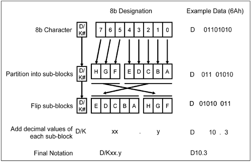
In Figure 11-15 on page 422, the example character is the Data character, 6Ah.
The bits in the character are identified by the capitalized alpha designators A through H.
The character is partitioned into two sub-blocks:
one 3-bits wide and the other 5-bits wide. The two sub-blocks are flipped. The character takes the written form Zxx.y, where: Z = D or K for Data or Control, xx = the decimal value of the 5-bit field, y = the decimal value of the 3-bit field. The example character is represented as D10.3 in the 8b/10b lookup tables.
Disparity
Definition
Character disparity refers to the difference between the number of 1s and 0s in a 10-bit symbol:
When a symbol has more 0s than 1s, the symbol has negative (–) disparity (e.g., 0101000101b). When a symbol has more 1s than 0s, the symbol has positive (+) disparity (e.g., 1001101110b). When a symbol has an equal number of 1s and 0s, the symbol has neutral disparity (e.g., 0110100101b). Each 10-bit symbol contains one of the following numbers of ones and zeros (not necessarily contiguous): Four 0s and six 1s (+ disparity). Six 0s and four 1s (– disparity). Five 0s and five 1s (neutral disparity).
Two Categories of 8-bit Characters
There are two categories of 8-bit characters:
CRD (Current Running Disparity)
The CRD reflects the total number of 1s and 0s transmitted over the link since link initialization and has the following characteristics:
Its current state indicates the balance of 1s and 0s transmitted since link initialization. The CRD's initial state (before any characters are transmitted) can be + or –. The CRD's current state can be either positive (if more 1s than 0s have been transmitted) or negative (if more 0s than 1s). Each character is converted via a table lookup with the current state of the CRD factored in. As each new character is encoded, the CRD either remains the same (if the newly generated 10-bit character has neutral disparity) or it flips to the opposite polarity (if the newly generated character has + or – disparity).
8b/10b Encoding Procedure
Refer to Figure 11-16 on page 425. The encode is accomplished by performing two table lookups in parallel (not shown separately in the illustration):
First Table Lookup:
Three elements are submitted to a 5-bit to 6-bit table for a lookup (see Table 11-1 on page 427 and Table 11-2 on page 429): - The 5-bit portion of the 8-bit character (bits A through E). - The Data/Control (D/K#) indicator. - The current state of the CRD (positive or negative). - The table lookup yields the upper 6-bits of the 10-bit symbol (bits abcdei).
Second Table Lookup:
Three elements are submitted to a 3-bit to 4-bit table for a lookup (see Table 11-3 on page 429 and Table 11-4 on page 430): - The 3-bit portion of the 8-bit character (bits F through H). - The same Data/Control (D/K#) indicator. - The current state of the CRD (positive or negative). - The table lookup yields the lower 4-bits of the 10-bit symbol (bits fghj).
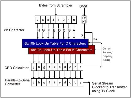
The 8b/10b encoder computes a new CRD based on the resultant 10-bit symbol and supplies this CRD for the 8b/10b encode of the next character. If the resultant 10-bit symbol is neutral (i.e., it has an equal number of 1s and 0s), the polarity of the CRD remains unchanged. If the resultant 10-bit symbol is + or –, the CRD flips to its opposite state. It is an error if the CRD is currently + or – and the next 10-bit symbol produced has the same polarity as the CRD (unless the next symbol has neutral disparity, in which case the CRD remains the same).
The 8b/10b encoder feeds a Parallel-to-Serial converter which clocks 10-bit symbols out in the bit order 'abcdeifghj' (shown in Figure 11-16 on page 425).
Example Encodings
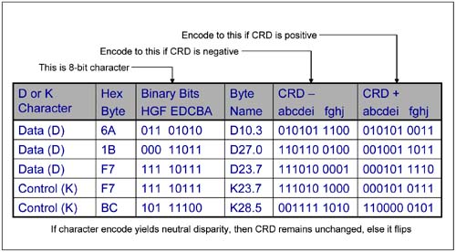
Figure 11-17 on page 426 illustrates some example 8-bit to 10-bit encodings. The following is an explanation of the conversion of the 8-bit Data character 6Ah:
The 8-bit character is broken down into its two sub-blocks:
011b and 01010b. The two sub-blocks are flipped and represented as the D10.3 character. The binary-weighted value of the 5-bit block is 10d and the value of the 3-bit field is 3d. The two blocks are submitted to the data character lookup tables (Table 11-1 on page 427 and Table 11-3 on page 429 are for D lookups) along with the current state of the CRD). The last two columns show the 10-bit symbol produced by the two parallel table lookups (Table 11-1 on page 427 and Table 11-3 on page 429) when the CRD is negative or positive.
Example Transmission
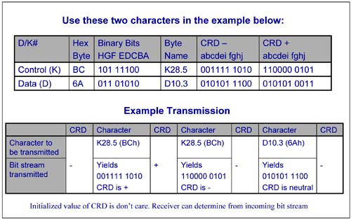
Figure 11-18 on page 427 illustrates the encode and transmission of three characters: the first one is the control character BCh (K28.5), the second character is also BCh (K28.5) and the third character is the data character 6Ah (D10.3):
If the initial CRD is negative at the time of the encode, the K28.5 is encoded into 001111 1010b (positive disparity), flipping the CRD from negative to positive. If the CRD is positive at the time of the encode, the K28.5 is encoded into 110000 0101b (negative disparity), flipping the CRD from positive to negative. The D10.3 is encoded into 010101 1100b (neutral disparity). The CRD therefore remains unchanged (negative) for the next encoding (not shown). Notice that the resultant symbol stream is DC balanced.
The Lookup Tables
The following four tables define the table lookup for the two sub-blocks of 8-bit Data and Control characters.
Table 11-1. 5-bit to 6-bit Encode Table for Data Characters|
D0 | 00000 | 100111 | 011000 | D1 | 00001 | 011101 | 100010 | D2 | 00010 | 101101 | 010010 | D3 | 00011 | 110001 | 110001 | D4 | 00100 | 110101 | 001010 | D5 | 00101 | 101001 | 101001 | D6 | 00110 | 011001 | 011001 | D7 | 00111 | 111000 | 000111 | D8 | 01000 | 111001 | 000110 | D9 | 01001 | 100101 | 100101 | D10 | 01010 | 010101 | 010101 | D11 | 01011 | 110100 | 110100 | D12 | 01100 | 001101 | 001101 | D13 | 01101 | 101100 | 101100 | D14 | 01110 | 011100 | 011100 | D15 | 01111 | 010111 | 101000 | D16 | 10000 | 011011 | 100100 | D17 | 10001 | 100011 | 100011 | D18 | 10010 | 010011 | 010011 | D19 | 10011 | 110010 | 110010 | D20 | 10100 | 001011 | 001011 | D21 | 10101 | 101010 | 101010 | D22 | 10110 | 011010 | 011010 | D23 | 10111 | 111010 | 000101 | D24 | 11000 | 110011 | 001100 | D25 | 11001 | 100110 | 100110 | D26 | 11010 | 010110 | 010110 | D27 | 11011 | 110110 | 001001 | D28 | 11100 | 001110 | 001110 | D29 | 11101 | 101110 | 010001 | D30 | 11110 | 011110 | 100001 | D31 | 11111 | 101011 | 010100 |
Table 11-2. 5-bit to 6-bit Encode Table for Control Characters|
K28 | 11100 | 001111 | 110000 | K23 | 10111 | 111010 | 000101 | K27 | 11011 | 110110 | 001001 | K29 | 11101 | 101110 | 010001 | K30 | 11110 | 011110 | 100001 |
Table 11-3. 3-bit to 4-bit Encode Table for Data Characters|
--.0 | 000 | 1011 | 0100 | --.1 | 001 | 1001 | 1001 | --.2 | 010 | 0101 | 0101 | --.3 | 011 | 1100 | 0011 | --.4 | 100 | 1101 | 0010 | --.5 | 101 | 1010 | 1010 | --.6 | 110 | 0110 | 0110 | --.7 | 111 | 1110/0111 | 0001/1000 |
Table 11-4. 3-bit to 4-bit Encode Table for Control Characters|
--.0 | 000 | 1011 | 0100 | --.1 | 001 | 0110 | 1001 | --.2 | 010 | 1010 | 0101 | --.3 | 011 | 1100 | 0011 | --.4 | 100 | 1101 | 0010 | --.5 | 101 | 0101 | 1010 | --.6 | 110 | 1001 | 0110 | --.7 | 111 | 0111 | 1000 |
Control Character Encoding
Table 11-5 on page 432 shows the encoding of the PCI Express-defined Control characters. These characters are not scrambled by the transmitter logic, but are encoded into 10-bit symbols. Because these Control characters are not scrambled, the receiver logic can easily detect these symbols in an incoming symbol stream.
These Control characters have the following properties
COM (comma) character.
The COM character is used as the first character of any Ordered-Set. Ordered-Sets are a collection of multiples of 4 characters that are used for specialized purposes (see "Ordered-Sets" on page 433). The 10-bit encoding of the COM (K28.5) character contains two bits of one polarity followed by five bits of the opposite polarity (001111 1010 or 110000 0101). The COM (and FTS) symbols are the only two symbols that have this property, thereby making it easy to detect at the receiver's Physical Layer. A receiver detects the COM pattern to detect the start of an Ordered-Set. In particular, the COM character associated with TS1, TS2, or FTS Ordered-Sets are used by a receiver to achieve bit and symbol lock on the incoming symbol stream. See "Link Training and Initialization" on page 403 for more details.
PAD character.
On a multi-Lane Link, assume the transmitter transmits the END character associated with a packet end on an intermediate Lane such as Lane 3 of a x8 Link. If the Link goes to the Logical Idle state after the transmission of the packet's END character, then the PAD character is used to fill in the remaining Lanes. This is done so packets as well as Logical Idle sequences always begin on Lane 0. For more information, see "x8, x12, x16 or x32 Packet Format Rules" on page 413 and "x8 Packet Format Example" on page 415.
SKP (skip) character.
The SKP character is used as part of the SKIP Ordered-Set. The SKIP Ordered-Set is transmitted for clock tolerance compensation. For a detailed description, refer to "Inserting Clock Compensation Zones" on page 436 and "Receiver Clock Compensation Logic" on page 442.
STP (Start TLP) character.
This character is inserted to identify the start of a TLP.
SDP (Start DLLP) character.
This character is inserted to identify the start of a DLLP.
END character.
This character is inserted to identify the end of a TLP or DLLP that has not experienced any CRC errors on previously-traversed links.
EDB (EnD Bad packet) character.
This character is inserted to identify the end of a TLP that a forwarding device (such as a switch) wishes to 'nullify'. Cut-through mode is a mode in which the switch forwards a packet from its ingress port to an egress port with minimal latency without having to buffer the incoming packet first. A switch may have started forwarding a packet in cut-through mode and then discovered that the packet is corrupted. It therefore must instruct the receiver of this packet to discard it. To nullify a TLP, the switch ends the packet with the EDB character and inverts the LCRC from its calculated value. A receiver that receives such a nullified packet discards it and does not return an ACK or NAK. Also see the chapter on Ack/Nak for a detailed description of the switch cut-through mode.
FTS (Fast Training Sequence) character.
This character is used as part of the FTS Ordered-Set. FTS Ordered-Sets are transmitted by a device in order to transition a Link from the low power L0s low power state back to the full-on L0 state.
IDL (Idle) character.
This character is used as part of the Electrical Idle Ordered-Set. The Ordered-Set is transmitted to inform the receiver that the Link is about to transition to the L0s low power state (also referred to as the Electrical Idle state of the Link).
Table 11-5. Control Character Encoding and Definition|
COM | K28.5 (BCh) | 001111 1010 | 110000 0101 | First character in any Ordered-Set. Detected by receiver and used to achieve symbol lock during TS1/TS2 Ordered-Set reception at receiver | PAD | K23.7 (F7h) | 111010 1000 | 000101 0111 | Packet Padding character | SKP | K28.0 (1Ch) | 001111 0100 | 110000 1011 | Used in SKIP Ordered-Set. This Ordered-Set is used for Clock Tolerance Compensation | STP | K27.7 (FBh) | 110110 1000 | 001001 0111 | Start of TLP character | SDP | K28.2 (5Ch) | 001111 0101 | 110000 1010 | Start of DLLP character | END | K29.7 (FDh) | 101110 1000 | 010001 0111 | End of Good Packet character | EDB | K30.7 (FEh) | 011110 1000 | 100001 0111 | Character used to mark the end of a 'nullified' TLP. | FTS | K28.1 (3Ch) | 001111 1001 | 110000 0110 | Used in FTS Ordered-Set. This Ordered-Set used to exit from L0s low power state to L0 | IDL | K28.3 (7Ch) | 001111 0011 | 110000 1100 | Used in Electrical Idle Ordered-Set. This Ordered-Set used to place Link in Electrical Idle state |
Ordered-Sets
General
Ordered-Sets are Physical Layer Packets (PLPs) consisting of a series of characters starting with the COM character and consisting a total of four characters. When transmitted, they are transmitted on all Lanes. Ordered-Sets are used for special functions such as:
The PCI Express specification defines five Ordered-Sets:
Training Sequence 1 (TS1), Training Sequence 2 (TS2), SKIP, Fast Training Sequence (FTS) and Electrical IDLE Ordered-Sets.
A brief description of each Ordered-Set follows.
TS1 and TS2 Ordered-Sets
These two Ordered-Sets are used during Link training. They are transmitted by a port's transmitter to the other port's receiver, where they are used to achieve bit and symbol lock. They are also used by the ports at opposite ends of a Link to number their Links and Lanes. These Ordered-Sets are used during Link speed and width negotiation.
SKIP Ordered-Set
In a multi-lane implementation, the SKIP Ordered-Set is periodically transmitted on all Lanes to allow the receiver clock tolerance compensation logic to compensate for clock frequency variations between the clock used by the transmitting device to clock out the serial bit stream and the receiver device's local clock. The receiver adds a SKP symbol to a SKIP Ordered-Set in the receiver elastic buffer to prevent a potential buffer underflow condition from occurring due to the transmitter clock being slower than the local receiver clock. Alternately, the receiver deletes a SKP symbol from the SKIP Ordered-Set in the receiver elastic buffer to prevent a potential buffer overflow condition from occurring due to the transmitter clock being faster than the local receiver clock. For a detailed description, refer to "Inserting Clock Compensation Zones" on page 436 and "Receiver Clock Compensation Logic" on page 442.
Electrical Idle Ordered-Set
A transmitter device that wishes to place the Link in the Electrical Idle state (aka the L0s low power state) transmits this Ordered-Set to a receiver. Upon receipt, the differential receivers prepare for this low power state during which the transmitter driver can be in the low- or high-impedance state and packet transmission stops. The differential receiver remains in the low-impedance state while in this state.
FTS Ordered-Set
FTS Ordered-Sets are transmitted by a device to transition a Link from the low power L0s state back to the full-on L0 state. The receiver detects the FTS Ordered-Set and uses it to achieve bit and symbol lock as well as to re-synchronize its receiver PLL to the transmitter clock used to transmit the serial bit stream. See the Link Training and Power Management chapters for more details on FTS Ordered-Set usage.
Parallel-to-Serial Converter (Serializer)
The 8b/10b Encoder on each Lane feeds the Parallel-to-Serial converter associated with that Lane. The Parallel-to-Serial converter clocks 10-bit symbols out in the bit order 'abcdeifghj', with the least significant bit (a) shifted out first and the most significant bit (j) shifted out last (as shown in Figure 11-16 on page 425). The symbols supplied by the 8b/10b Encoder are clocked into the converter at 250MHz. The serial bit stream is clocked out of the Parallel-to-Serial converter at 2.5GHz.
Differential Transmit Driver
The differential driver that actually drives the serialized bit stream onto the wire (or fiber) uses NRZ encoding and drives the serial bit stream at the 2.5Gbit/s transfer rate. The differential driver output per Lane consists of two signals (D+ and D-). A logical one is signaled by driving the D+ signal high and the D- signal low, thus creating a positive voltage difference between the D+ and D- signals. A logical zero is signaled by driving the D+ signal low and the D- signal high, thus creating a negative voltage difference between the D+ and D- signals.
Differential peak-to-peak voltage driven by the transmitter is between 800mV (min.) and 1200mV (max).
During the Link's electrical Idle state, the transmitter drives a differential peak voltage between 0mV and 20mV (the transmitter may be in the low- or high-impedance state).
Details regarding the electrical characteristics of the driver are discussed in "Transmitter Driver Characteristics" on page 477
Transmit (Tx) Clock
The serial output of the Parallel-to-Serial converter on each Lane is clocked out to the differential driver by the Tx Clock signal (see Figure 11-16 on page 425). Tx clock frequency is 2.5GHz and it must be accurate to +/–300ppm from a center frequency of 2.5GHz (or 600ppm total). The clock can skew by one clock every 1666 clock cycles. Note that this Tx Clock is different from the local clock of the Physical Layer which is a much slower clock. The Physical Layer receives a clock from an external source. PCI Express devices on peripheral cards as well as system boards may use a 100MHz clock supplied by the system board. This clock is multiplied by a factor with the aid of a PLL internal to the Physical Layer. The resultant local clock, which runs at a much slower frequency than 2.5GHz, clocks Physical Layer logic such as the Byte Striping logic, the Scrambler, the 8b/10b Encoder, the buffers, etc. The PLL also produces the 2.5GHz Tx clock used to feed the Parallel-to-Serial converters.
Other Miscellaneous Transmit Logic Topics
Logical Idle Sequence
In order to keep the receiver's PLL sync'd up (i.e., to keep it from drifting), something must be transmitted during periods when there are no TLPs, DLLPs or PLPs to transmit. The logical Idle sequence is transmitted during these times. The Idle sequence is gated to the Mux as described in the section "Multiplexer (Mux) and Mux Control Logic" on page 404. Some properties of the Logical Idle sequence are:
The logical Idle sequence consists of the 8-bit Data character with a value of 00h. When transmitted, it is simultaneously transmitted on all Lanes. The Link is said to be in the logical Idle state (not to be confused with electrical Idle—the state when the Link is not driven and there are no packet transmissions and the receiver PLL loses synchronization). The logical Idle sequence is scrambled. This implies that, on the Link, the logical Idle sequence has a pseudo-random value. A receiver can distinguish the logical Idle sequence from other packet transmissions because it occurs outside the packet framing context (i.e., the logical Idle sequence occurs after an END or EDB Control symbol, but before an STP or SDP Control symbol). The logical Idle Sequence is 8b/10b encoded. During Logical Idle sequence transmission, SKIP Ordered-Sets are also transmitted periodically.
Inserting Clock Compensation Zones
Background
When the receiver logic receives a symbol stream, it sometimes needs to add or remove a symbol from the received symbol stream to compensate for transmitter verses receiver clock frequency variations (for background, refer to "Receiver Clock Compensation Logic" on page 442).
It should be obvious that the receiver logic can't arbitrarily pick a symbol to add or delete. This means that, on a periodic basis, the transmit logic must transmit a special Control character sequence that can be used for this purpose. This sequence is referred to as the SKIP Ordered-Set (see Figure 11-19) which consists of a COM character followed by three SKP characters.

SKIP Ordered-Set Insertion Rules
A transmitter is required to transmit SKIP Ordered-Sets on a periodic basis. The following rules apply:
The set must be scheduled for insertion at most once every 1180 symbol clocks (i.e., symbol times) and at least once every 1538 symbol clocks. When it's time to insert a SKIP Ordered-Set, it is inserted at the next packet boundary (not in the middle of a packet). SKIP Ordered-Sets are inserted between packets simultaneously on all Lanes. If a long packet transmission is already in progress, the SKIP Ordered-Sets are accumulated and then inserted consecutively at the next packet boundary. In a multi-Lane environment, the SKIP Ordered-Set must be transmitted on all Lanes simultaneously (see Figure 11-11 on page 414 and Figure 11-12 on page 415). When necessary, the Link is padded so as to allow all the transmission of the SKIP Ordered-Sets to start on the same clock (see Figure 11-12 on page 415). During all lower power Link states, any counter(s) used to schedule SKIP Ordered-Sets must be reset. SKIP Ordered-Sets must not be transmitted while the Compliance Pattern is in progress.
|

