| [ Team LiB ] |


|
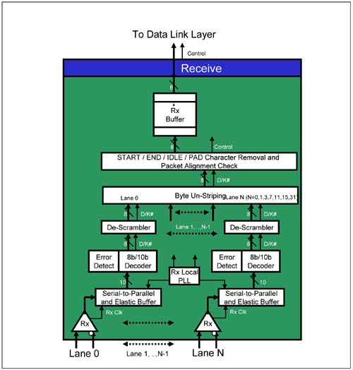
Receive Logic DetailsFigure 11-20 shows the receiver logic of the Logical Physical Layer. This section describes packet processing from the time the data is received serially on each Lane until the packet byte stream is clocked to the Data Link Layer. Figure 11-20. Physical Layer Receive Logic Details
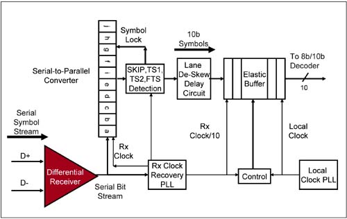
Figure 11-21 illustrates the receiver logic's front end on each Lane. This is comprised of:
Figure 11-21. Receiver Logic's Front End Per Lane
Differential ReceiverRefer to Figure 11-21. The differential receiver on each Lane senses differential peak-to-peak voltage differences > 175 mV but < 1200 mV:
A signal peak-to-peak difference < 65 mV is considered a signal absent condition and the Link is in the electrical Idle state. During this time, the receiver de-gates its input to prevent the error circuit from detecting an error. A signal peak-to-peak differential voltage between 65mV and 175mV serves as noise guard band. Rx Clock RecoveryGeneralUsing a PLL (Phase-Locked Loop), the receiver circuit generates the Rx Clock from the data bit transitions in the input data stream. This recovered clock has the same frequency (2.5GHz) as that of the Tx Clock used by the transmitting device to clock the data bit stream onto the wire (or fiber). The Rx Clock is used to clock the inbound serial symbol stream into the Serial-to-Parallel converter (Deserializer). The 10-bit symbol stream produced by the Deserializer is clocked into the elastic buffer with a divide by 10 version of the Rx Clock. The Rx Clock is different from the Local Clock that is used to clock symbols out of the Elastic Buffer to the 10b/8b decoder. The Local Clock must be accurate to within +/–300ppm from center frequency. Achieving Bit LockRecollect that the inbound serial symbol stream is guaranteed to have frequent 1-to-0 and 0-to-1 transitions due to the 8b/10b encoding scheme. A transition is guaranteed at least every 5 bit-times. The receiver PLL uses the transitions in the received bit-stream to synchronize the Rx Clock with the Tx Clock that was used at the transmitter to clock out the serialized bit stream. When the receiver PLL locks on to the Tx Clock frequency, the receiver is said to have achieved "Bit Lock". During Link training, the transmitter device sends a long series of back-to-back TS1 and TS2 Ordered-Sets to the receiver and the receiver uses the bit transitions in these Ordered-Sets to achieve Bit Lock. Once the Link is in the full-on L0 state, transitions on the Link occur on a regular basis and the receiver PLL is able to maintain Bit Lock. Losing Bit LockIf the Link is put in a low power state (such as L0s) where packet transmission ceases, the receiver's PLL gradually loses synchronization. The transmitter sends an electrical Idle Ordered-Set to tell the receiver to de-gate its input to prevent the error circuit from detecting an error. Regaining Bit LockWhen the Link is in the L0s state, the transmitter sends a few FTS Ordered-sets (on the order of four FTSs) to the receiver and the receiver uses these to regain Bit Lock. Only a few FTSs are needed by the receiver in order to achieve Bit Lock (thus the wake up latency is of short duration). Because the Link is in the L0s state for a short time, the receiver PLL does not completely lose synchronization with the Tx Clock before it receives the FTSs. Serial-to-Parallel converter (Deserializer)The incoming serial data on each Lane is clocked into that Lane's Deserializer (the serial-to-parallel converter) by the Rx clock (see Figure 11-21 on page 439). The 10-bit symbols produced are clocked into an Elastic Buffer using a divide-by-10 version of the Rx Clock. Symbol Boundary Sensing (Symbol Lock)When the receive logic starts receiving a bit stream, it is JABOB (just a bunch of bits) with no markers to differentiate one symbol from another. The receive logic must have some way to determine the start and end of a 10-bit symbol. The Comma (COM) symbol serves this purpose. The 10-bit encoding of the COM (K28.5) symbol contains two bits of one polarity followed by five bits of the opposite polarity (0011111010b or 1100000101b). Unless an error occurs, no other character has this property, thereby making it easily detectable. Recollect that the COM Control character, like all other Control characters, is not scrambled by the transmitter. This makes the COM easily detectable by the COM detector which looks for two consecutive 0s or two consecutive 1s followed by a string of five 1s or five 0s, respectively. Upon detection of the COM symbol, the COM Detector knows that the next bit received after the COM symbol is the first bit of a valid 10-bit symbol. The Deserializer is then initialized so that it can henceforth generate valid 10-bit symbols. The Deserializer is said to achieve 'Symbol Lock'. The COM symbol is utilized to achieve Symbol Lock under the following circumstances:
Receiver Clock Compensation LogicBackgroundConsider a transmitter at one end of a Link and the receiver at the opposite end. The transmit clock accuracy must be 2.5GHz +/– 300 ppm (parts per million). Once the Link is trained, the receive clock (Rx Clock) in the receiver is the same as the transmit clock (Tx Clock) at the other end of the Link (because the receive clock is derived from the bit stream that was transmitted at the remote end's transmit clock frequency). If the transmitter's Tx Clock at one end of the Link operates at +300 ppm and the Local Clock (shown in Figure 11-21 on page 439—not the Rx Clock) at the receiver at the other end operates at –300 ppm, this results in a worst-case 600 ppm difference between the two clocks. In this scenario, the transmitter at one end of the Link is operating at 2.5GHz +300 ppm, while the receiver's local clock is operating at a frequency of 2.5GHz – 300ppm. The Tx Clock of the transmitter and Local Clock of the receiver can therefore shift one clock every 1666 clocks. The Elastic Buffer's Role in the ReceiverIt is a common design practice to clock most of the receive path logic using the Physical Layer's local clock. To compensate for the frequency difference between the Rx Clock (which is derived from the remote port's transmit frequency) and the Local Clock (which is derived from the local port's transmit frequency), an elastic buffer (see Figure 11-21 on page 439) is incorporated in the very early stages of the receive path. Symbols arrive at the differential receiver as a bit stream and are presented to the Deserializer. The receive PLL recovers the clock (Rx Clock) embedded in the bit stream and the Deserializer converts the incoming bit stream into a series of 10-bit symbols. The symbols are clocked into the input side of the Elastic Buffer using the Rx Clock recovered from the incoming bit stream and are clocked out of the buffer using the receiver's local clock. As previously cited, these two clocks can be as much as 600ppm out of sync with each other. The Elastic Buffer compensates for the difference between the two clocks by either deleting a SKP symbol from or inserting a SKP symbol into the symbols contained in the Elastic Buffer:
The transmitter on the other end periodically transmits a special symbol sequence called the SKIP Ordered-Set (see Figure 11-19 on page 437 and "Inserting Clock Compensation Zones" on page 436) from which the "don't care" SKP symbol can be deleted or to which a "don't care" SKP symbol can be added. The SKIP Ordered-Set consists of four control symbols (a COM and three SKPs; the Skips are the "don't care" characters, hence the name "Skip"). Deleting or adding a SKP symbol to the SKIP Ordered-Set in the Elastic Buffer prevents a buffer overflow or underflow condition, respectively. Loss of symbol(s) caused by Elastic Buffer overflow or underflow triggers a Receiver Error indication to the Data Link Layer and results in the automatic initiation of Link error recovery. The transmitter schedules a SKIP Ordered-Set transmission once every 1180 to 1538 symbol times. However, if the transmitter starts a maximum sized TLP transmission right at the 1538 symbol time boundary when a SKIP Ordered-Set is scheduled to be transmitted, the SKIP Ordered-Set transmission is deferred. Receivers must be tolerant to receive and process SKIP Ordered-Sets that have a maximum separation dependent on the maximum packet payload size a device supports. The formula for the maximum number of Symbols (n) between SKIP Ordered-Sets is: n = 1538 + (maximum packet payload size + 26) 26 is the number of symbols associated with the header (16 bytes), the optional ECRC (4 bytes), the LCRC (4 bytes), and the sequence number (2 bytes). Lane-to-Lane De-SkewNot a Problem on a Single-Lane LinkThe problem of Lane-to-Lane skew is obviously only an issue on multi-Lane Links. Flight Time Varies from Lane-to-LaneSymbols are transmitted simultaneously on all Lanes using the same transmit clock, but they cannot be expected to arrive at the receiver at the same time (i.e., without Lane-to-Lane skew). A multi-Lane Link may have many sources of Lane-to-Lane skew. These sources include but are not limited to:
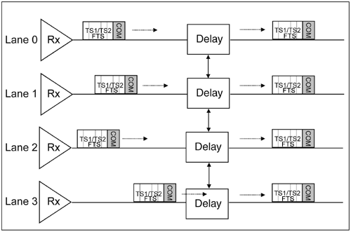
When the byte-striped serial bit streams associated with a packet arrive on all Lanes at the receiver, it must remove this Lane-to-Lane skew in order to receive and process the data correctly. This process is referred to as Link deskew. Receivers use TS1 or TS2 Ordered-Sets during Link training or FTS Ordered-Sets during L0s exit to perform Link de-skew functions. If Lane Data Is Not Aligned, Byte Unstriping Wouldn't WorkHavoc would ensue if the symbols transmitted on each Lane simultaneously were to arrive at each Lane receiver at different times and were then de-serialized and fed to the Byte Unstriping Logic. Gibberish would be fed to the Link Layer as packet data. TS1/TS2 or FTS Ordered-Sets Used to De-Skew LinkThe unique structure and length of the TS1/TS2 and FTS sets, and the fact that they are transmitted simultaneously on all Lanes, are used by the receiver's De-Skew logic to determine the amount of misalignment between Lanes. The specification doesn't define the method used to achieve multi-Lane alignment. As an example, the receiver logic could compensate for the misalignment by tuning an automatic delay circuit in each Lane's receiver (see Figure 11-21 on page 439 and Figure 11-22 on page 445). Figure 11-22. Receiver's Link De-Skew Logic
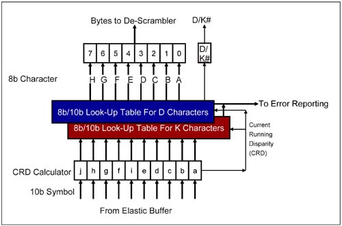
The receiver must be capable of de-skewing up to 20ns of Lane-to-Lane skew as defined by the LRX-SKEW parameter shown in Table 12-2 on page 480. De-Skew During Link Training, Retraining and L0s ExitTS1 and TS2 Ordered-Sets are only transmitted during initial Link training or during Link retraining (i.e., recovery). FTS Ordered-Sets are transmitted during L0s exit. De-skew is therefore only performed by the receiver at those times and is not done on a periodic basis. Lane-to-Lane De-Skew Capability of ReceiverThe Lane-to-Lane de-skew parameter LRX-SKEW shown in Table 12-2 on page 480 requires that the receiver be capable of de-skewing Lane delays of up to 20ns. The transmitter is allowed to introduce a minimal Lane-to-Lane skew at the output pad defined by the LTX-SKEW parameter (see Table 12-1 on page 477) of 1.3ns. 8b/10b DecoderGeneralRefer to Figure 11-23 on page 447. Each receiver Lane incorporates a 10b/8b Decoder which is fed from the Elastic Buffer. The 8b/10b Decoder uses two lookup tables (the D and K tables) to decode the 10-bit symbol stream into 8-bit Data (D) or Control (K) characters plus the D/K# signal. The state of the D/K# signal indicates that the received symbol is:
Figure 11-23. 8b/10b Decoder per Lane
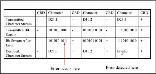
Disparity CalculatorThe decoder determines the initial disparity value based on the disparity of the first symbol received. After the first symbol, once the disparity is initialized in the decoder, it expects the calculated disparity for each subsequent symbol received to toggle between + and - unless the symbol received has neutral disparity in which case the disparity remains the same value. Code Violation and Disparity Error DetectionGeneralThe error detection logic of the 8b/10b Decoder detects errors in the received symbol stream. It should be noted that it doesn't catch all possible transmission errors. The specification requires that these errors be detected and reported as a Receiver Error indication to the Data Link Layer. The two types of errors detected are:
There is no automatic hardware error correction for these errors at the Physical Layer. Code ViolationsThe following conditions represent code violations:
Disparity ErrorsA character that encodes into a 10-bit symbol with disparity other than neutral is encoded into a 10-bit symbol with polarity opposite to that of the CRD. If the next symbol does not have neutral disparity and its disparity is the same as the CRD, a disparity error is detected.
De-ScramblerThe De-Scrambler is fed by the 8b/10b Decoder block. The De-Scrambler only de-scrambles Data (D) characters associated with a TLP or DLLP (D/K# is high). It does not de-scramble Control (K) characters or Ordered-Sets. K characters and Ordered-Sets sourced from the 8b/10b decoder are valid as is. Some De-Scrambler Implementation Rules:
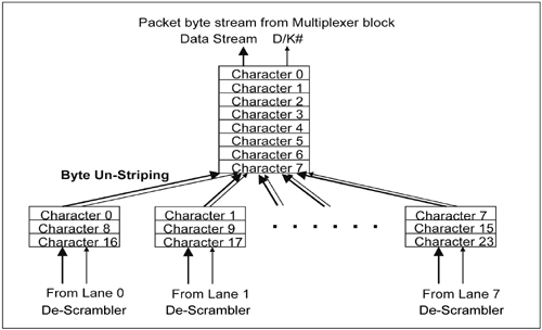
Disabling De-ScramblingIf the receiver De-Scrambler receives at least two TS1/TS2 Ordered-Sets with the disable scrambling bit set from the remote device on all of its configured Lanes, it disables its De-Scrambler. Byte Un-StripingFigure 11-25 on page 449 illustrates an example of eight decoded 8-bit character streams from the eight De-Scramblers of a x8 Link being un-striped into a single byte stream which is fed to the Filter logic (see the next section). Figure 11-25. Example of x8 Byte Un-Striping
Filter and Packet Alignment CheckThe serial byte stream supplied by the byte un-striping logic contains TLPs, DLLPs, Logical Idle sequences, Control characters such as STP, SDP, END, EDB, and PADs, as well as the types of Ordered-Sets. Of these characters, the Logical Idle sequence, the control characters and Ordered-Sets are detected and eliminated. What remains are TLPs and DLLPs which are sent to the Rx Buffer along with boundary characters indicating the start and end of each TLP and DLLP. Receive Buffer (Rx Buffer)The Rx Buffer holds received TLPs and DLLPs after the start and end characters have been eliminated. The received packets are ready to send to the Data Link Layer. The interface between the Physical Layer and Data Link Layer is unspecified. Hence, the designer is free to decide what data bus width interface to implement. As an example, we can assume the interface clock to be 250MHz. In that case, the width of the data bus connecting the Data Link Layer to the Physical Layer interface can = the number of Lanes supported by the device x eight bits.  |
| [ Team LiB ] |
|