| [ Team LiB ] |


|
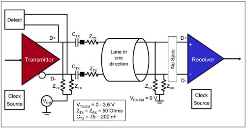
High Speed Electrical SignalingRefer to Figure 12-2. High-speed LVDS (Low-Voltage Differential Signaling) electrical signaling is used in driver and receiver implementations. Drivers and receivers from different manufacturers must be inter-operable and may be designed to be hot-pluggable. A standard FR4 board can be used to route the Link wires. The following sections describe the electrical characteristics of the driver, receiver, and the Link represented in the Figure. Figure 12-2. Differential Transmitter/Receiver
Clock RequirementsGeneralThe transmitter clocks data out at 2.5Gbits/s. The clock used to do so must be accurate to +/- 300 ppm of the center frequency. It is allowed to skew a maximum of 1 clock every 1666 clocks. The two devices at the opposite ends of a Link could have their transmit clocks out of phase by as much as 600 ppm. A device may derive its clock from an external clock source. The system board supplies a 100 MHz clock that is made available to devices on the system board as well as to add-in cards via the connector. With the aid of PLLs, a device may generate its required clocks from this 100 MHz clock. Spread Spectrum Clocking (SSC)Spread spectrum clocking is a technique used to modulate the clock frequency slowly so as to reduce EMI radiated noise at the center frequency of the clock. With SSC, the radiated energy does not produce a noise spike at 2.5GHz because the radiated energy is spread over a small frequency range around 2.5GHz. SCC is not required by the specification. However, if supported, the following rules apply:
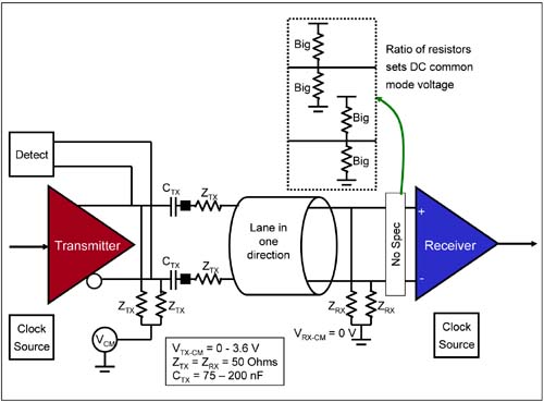
Impedance and TerminationThe characteristic impedance of the Link is 100 Ohms differential (nominal), while single-ended DC common mode impedance is 50 Ohms. This impedance is matched to the transmitter and receiver impedances. Transmitter Impedance RequirementsTransmitters must meet the ZTX-DIFF-DC (see Table 12-1 on page 477) parameters anytime differential signals are transmitted during the full-on L0 power state. When a differential signal is not driven (e.g., in the lower power states), the transmitter may keep its output impedance at a minimum ZTX-DC (see Table 12-1 on page 477) of 40 Ohms, but may also place the driver in a high impedance state. Placing a driver in the high impedance state may be helpful while in L0s or L1 low power states to help reduce power drain in these states. Receiver Impedance RequirementsThe receiver is required to meet the ZRX-DIFF-DC (see Table 12-2 on page 480) parameter of 100 Ohms anytime differential signals are transmitted during the full-on L0 power state, as well as in all other lower power states wherein adequate power is provided to the device. A receiver is excluded from this impedance requirement when the device is powered down (e.g., in the L2 and L3 power states and during Fundamental Reset). When a receiver is powered down to the L2 or L3 state, or during Fundamental Reset, its receiver goes to the high impedance state and must meet the ZRX-HIGH-IMP-DC parameter of 200 KOhms minimum (see Table 12-2 on page 480). DC Common Mode VoltagesTransmitter DC Common Mode VoltageOnce driven after power-on and during the Detect state of Link training, the transmitter DC common mode voltage VTX-DC-CM (see Table 12-1 on page 477) must remain at the same voltage. The common mode voltage is turned off only when the transmitter is placed in the L2 or L3 low power state, during which main power to the device is removed. A designer can choose any common mode voltage in the range of 0V to 3.6V. Receiver DC Common Mode VoltageThe receiver is DC de-coupled from the transmitter by a capacitor. This allows the receiver to have its own DC common mode voltage. This voltage is specified at 0V. The specification is unclear about the meaning of this 0V receiver DC common mode voltage requirement and does not require the common mode voltage to be 0V at the input to the receiver differential amplifier. Rather, a simple bias voltage network allows the receiver to operate at optimal common mode. See Figure 12-3 on page 458. Figure 12-3. Receiver DC Common Mode Voltage Requirement
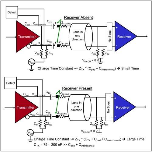
ESD and Short Circuit RequirementsAll signals and power pins must withstand (without damage) a 2000V Electro-Static Discharge (ESD) using the human body model and 500V using the charged device model. For more details on this topic, see the JEDEC JESE22-A114-A specification. The ESD requirement not only protects against electro-static damage, but facilitates support of surprise hot insertion and removal events. Transmitters and receivers are also required to be short-circuit tolerant. They must be able to withstand sustained short-circuit currents (on D+ or D- to ground) of ITX-SHORT (see Table 12-2 on page 480) in the order of 90mA (the maximum current a transmitter is required to provide). Receiver DetectionGeneralThe Detect block in the transmitter shown in Figure 12-2 on page 455 is required to detect the presence or absence of a receiver at the other end of the Link after coming out of reset or power-on. The Detect state of the Link Training state machine is responsible for making this determination. Detection is accomplished when the transmitter changes the DC common mode voltage from one value to another. By design, the transmitter detect logic has knowledge of the rate at which the lines charge with or without a receiver. With a Receiver AttachedWith a receiver attached at the other end of the Link, the charge time (RC time constant) is relatively long due to the large coupling capacitor (CTX). See the lower half of Figure 12-4 on page 460.
Figure 12-4. Receiver Detection Mechanism
Without a Receiver AttachedWithout a receiver attached at the other end of the Link, the charge time (RC time constant) is relatively short because the large coupling capacitor (CTX) does NOT come into play. See the upper half of Figure 12-4 on page 460.
Procedure To Detect Presence or Absence of Receiver
Differential Drivers and ReceiversDifferential signaling (as opposed to the single-ended signaling employed in PCI and PCI-X) is ideal for high frequency signaling. Advantages of Differential SignalingSome of the advantages of differential signaling (versus single-ended signaling) are:
Differential VoltagesThe differential driver uses NRZ encoding to drive the serial bit stream. The differential driver output consists of two signals, D+ and D-. A logical one is signaled by driving the D+ signal high and the D- signal low, creating a positive voltage difference between the D+ and D- signals. A logical Zero is signaled by driving the D+ signal low and the D- signal high, creating a negative voltage difference between the D+ and D- signals. The differential peak-to-peak voltage driven by the transmitter VTX-DIFFp-p (see Table 12-1 on page 477) is between 800 mV (minimum) and 1200 mV (max).
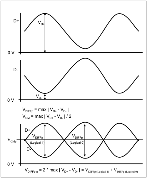
During the Link electrical Idle state, the transmitter drives a differential peak voltage VTX-IDLE-DIFFp (see Table 12-1 on page 477) of between 0 mV and 20 mV. In this state, the transmitter may be in the low-or high-impedance state. The receiver is able to sense a logical 1, a logical 0, as well as the electrical idle state of the Link by detecting the voltage on the Link via a differential receiver amplifier. Due to signal loss along the Link at high frequency, the receiver must be designed to sense an attenuated version of the differential signal driven by the transmitter. The receiver sensitivity is defined by the differential peak-to-peak voltage VRX-DIFFp-p (see Table 12-2 on page 480) of between 175 mV and 1200 mV. Differential Voltage NotationGeneralA differential signal voltage is defined by taking the difference in the voltage on the two conductors, D+ and D-. The voltage with respect to ground on each conductor is VD+ and VD-. The differential voltage is VDIFF = VD+ - VD-. The Common Mode voltage, VCM, is defined as the mean voltage of D+ and D-. VCM = (VD++ VD-) / 2. In defining differential voltages, the specification uses two parameters: 1) The differential peak-to-peak voltage, and 2) the Differential peak voltage. These voltages are defined by the following equations and are illustrated in Figure 12-5 on page 463.
Figure 12-5. Pictorial Representation of Differential Peak-to-Peak and Differential Peak Voltages
Differential Peak VoltageThe differential peak voltage is easily represented in a diagram as the differential voltage associated with signaling a logical 1 or logical 0. Differential Peak-to-Peak VoltageThe differential peak-to-peak voltage is not easily represented in a diagram. One can think of the differential peak-to-peak voltage as the sum total of the differential voltage for signaling a logical 1 and for signaling a logical 0. One can think of this voltage as the total voltage swing a receiver experiences between receiving a logical 1 and receiving a logical 0. Common Mode VoltageThe common mode voltage is the center voltage with respect to ground when the D+ and D- signals cross-over one another, assuming these two signals are symmetric. When a differential driver does not drive a differential voltage, it drives a common mode voltage with both D+ and D- signals at the same voltage (the signals do not swing). Electrical IdleThe electrical idle state of the Link is the state wherein the transmitter D+ and D- voltages are held at a steady, constant voltage (the common mode voltage). This state is used in power savings states such as L0s and L1, as well as the Link Inactive or Link Disable states. Transmitter ResponsibilityA transmitter that wishes to place a Link in the electrical Idle state must first transmit the electrical Idle Ordered-Set shown in Figure 12-6. After doing so, the transmitter must go to the electrical Idle state within TTX-IDLE-SET-TO-IDLE time (see Table 12-1 on page 477) which is less that 20 UI (Unit Intervals = 400ps, 20 UI = 8 ns). The differential peak voltage driven by the transmitter in the electrical Idle state is VTX-IDLE-DIFFp (see Table 12-1 on page 477) which is less than a 20mV peak. Figure 12-6. Electrical Idle Ordered-Set
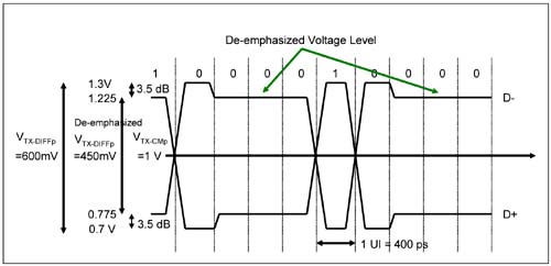
The transmitter can then remain in the low impedance state or go to the high impedance state. Once in the electrical Idle state, the transmitter must remain in this state for a minimum of TTX-IDLE-MIN (see Table 12-1 on page 477) which is 50 UI (20ns). To exit electrical Idle and return the Link to the full-on L0 state when transmission resumes, the transmitter must do so within TTX-IDLE-TO-DIFF-DATA (see Table 12-1 on page 477) which is less that 20 UI (8ns). The transmitter sends FTS Ordered-Sets or TS1/TS2 Ordered sets to transition the Link state from the L0s or L1 state, respectively, back to L0 full-on state. Receiver ResponsibilityA receiver determines that the Link is going to enter electrical Idle state when it sees two out of the three IDLs of the Ordered-Set. The receiver de-gates the error reporting logic to prevent reporting errors due to unreliable activity on the Link and also immediately arms its electrical Idle Exit detector. A receiver is able to detect an exit from the electrical Idle state when it detects a differential peak-to-peak voltage on the Link of greater than VRX-IDLE-DET-DIFFpp (see Table 12-2 on page 480) of 65mV. In the electrical Idle state, the receiver PLL will over time, lose clock synchronization because the receiver input is at a steady state voltage. To exit the electrical Idle state, a transmitter sends FTS or TS1/TS2 Ordered-Sets that the receiver uses to achieve Bit Lock and Symbol Lock and to resync the receiver PLL with the transmitter. Power Consumed When Link Is in Electrical Idle StateIn the electrical Idle state, the Link consumes less power because there are no Link voltage transitions that occur and the transmitter can de-gate its output stage. The Link is in either the L0s, L1, or the Disabled state while it remains in the electrical Idle state. The recommended power consumed in L0s is less than 20mW/Lane, while it is less than 5mW/Lane in the L1 state. The recommended power consumed per Lane in L0 is on the order of 80mW. Electrical Idle ExitA receiver detects electrical Idle exit when it receives a valid differential voltage within the VRX-DIFFp-p of 175 mV - 1200 mV. A transmitter typically sends TS1 Ordered-Sets to signal electrical Idle exit to a receiver. Transmission Line Loss on LinkThe transmitter drives a minimum differential peak-to-peak voltage VTX-DIFFp-p of 800mV. The receiver sensitivity is designed for a minimum differential peak-to-peak voltage (VRX-DIFFp-p) of 175 mV. This translates to a 13.2dB loss budget that a Link is designed for. Although a board designer can determine the attenuation loss budget of a Link plotted against various frequencies, the transmitter and receiver eye diagram measurement are the ultimate determinant of loss budget for a Link. Eye diagrams are described in "LVDS Eye Diagram" on page 470. A transmitter that drives up to the maximum allowed differential peak-to-peak voltage of 1200mV can compensate for a lossy Link that has worst-case attenuation characteristics. AC CouplingPCI Express requires AC coupling capacitors be placed in close proximity to the transmitter on each Lane's differential signal pair. The AC coupling capacitor, CTX (see Table 12-2 on page 480), is of a value between 75nF and 200nF. The capacitors can be integrated onto the system board, or integrated into the device itself. An add-in card with a PCI Express device on it must either place the capacitors on the card in close proximity to the transmitter, or integrate the capacitors into the PCI Express silicon. The AC coupling capacitors eliminate DC common mode voltage sharing between two devices at opposite ends of the Link. This simplifies the device design by allowing each device to operate with its own transmitter DC common voltage. Each device can operate with its own power and ground plane, independent of the remote device at the opposite end of the Link. De-Emphasis (or Pre-Emphasis)PCI Express employs the concept of de-emphasis to help reduce the effect of the inter-symbol interference that may occur, especially on more lossy Link transmission lines. Supporting this mandatory feature reduces the Bit Error Rate (BER). What is De-Emphasis?A transmitted differential signal is de-emphasized when multiple bits of the same polarity are transmitted back-to-back as shown in Figure 12-7 on page 467. The Figure show a transmission of '1000010000'. Some rules related to signal de-emphasis are:
Figure 12-7. Transmission with De-emphasis
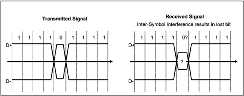
What is the Problem Addressed By De-emphasis?As bit transmission frequencies increase, the bit-time or Unit Interval (UI) decreases. At the 2.5GBit/s transmission rate, the Unit Interval is a very small (400ps). The capacitive effects on the Link transmission line become more apparent. The line capacitors (Cpad + Cinterconnect + CTX) store charge. When a signal has been held at a constant differential voltage (as in transmission of successive bits of the same polarity), the line capacitors charge up. The line does not easily change voltage when the signal polarity has to flip immediately to the opposite value. This results in what is referred to as inter-symbol interference. Consider the example in Figure 12-8 on page 468 wherein a transmitter sends the bit pattern '111101111'. The string of the first four logical 1s charges the line capacitors. When the transmitter follows this string with a logical 0, the capacitors cannot discharge fast enough and then charge to the opposite polarity, so that the receiver will register the logical 0. The result is inter-symbol interference at the receiver. A receiver eye diagram would show the 'lonely' logical 0 with a narrower eye. Figure 12-8. Problem of Inter-Symbol Interference
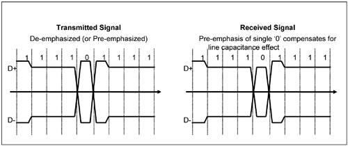
SolutionRather than thinking that each subsequent bit transmitted after the first bit of the same polarity must be de-emphasized by 3.5dB (the PCI Express specification prefers to use the term de-emphasis), think of the first bit of a string of same polarity bits as being pre-emphasized by 3.5dB. Consider the solution in Figure 12-9. By pre-emphasizing the 'lonely' logical 0 bit, the transmitter is given sufficient additional drive strength to overcome the capacitive effect of the previous string of logical 1s. Figure 12-9. Solution is Pre-emphasis
PCI Express device receivers are designed to detect differential signals that are attenuated by the Link transmission line by as much as 11-13.2dB from the transmitted value. The de-emphasis requirement for the transmitted signal is designed to accommodate systems with Link transmission lines that have this worst-case loss budget. Of course, for lower loss systems, there is more voltage margin at a receiver that receives a de-emphasized signal. Beacon SignalingGeneralA PCI Express device that is in the L2 low power state can generate a wake up event to inform the system that it wishes to move to the full-on L0 state. The Beacon signaling mechanism is one of two methods a device may employ to accomplish this. The other method (see "WAKE#" on page 696) is via the assertion of the WAKE# signal (if it is supported by the device). While a device is in the L2 power state, its main power source and clock are turned off (as described in "" on page 484). However, an auxiliary power source (Vaux) keeps a limited portion of the device powered, including the wake up signaling logic. When in the L2 low power state, a downstream device signals a Beacon wake up signal upstream to start the L2 exit sequence. If a switch or bridge receives the Beacon signal on its downstream port, it must forward the wake up event to its upstream port. This can be done by either forwarding the Beacon signal to the upstream port or by using WAKE# assertion to the power management logic. See "WAKE# (AUX Power)" on page 643. When a device's Link power state is L2, even though the main power to the device is powered off, a limited portion of the device is powered by Vaux. The powered portion of the device allows the device to signal the wake up event via the Beacon. An upstream device such as a switch, bridge or Root Complex that is also in L2 power state is able to sense the Beacon because the receiver Beacon signal detection logic is also powered by Vaux. Properties of the Beacon Signal
 |

| [ Team LiB ] |
|