PCI Express Extended Capabilities
General
A PCI Express function may optionally implement any, all, or none of the following Extended Capability register sets:
Advanced Error Reporting Capability register set. Virtual Channel (VC) Capability register set. Device Serial Number Capability register set. Power Budgeting Capability register set.
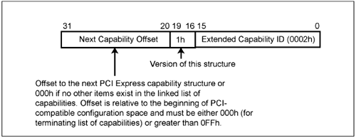
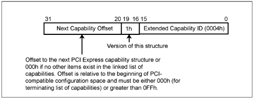
Refer to Figure 24-1 on page 895. The first extended capability register set must be implemented at offset 100h in a function's 4KB configuration space and its Enhanced Capability Header register (see Figure 24-15 on page 930) contains a pointer (the Next Capability Offset field; this 12-bit field must contain either the dword-aligned start address of the next capability register set, or a value of zero if this is the last of the extended capability register sets) to the next extended capability register set in the list. The respective capability IDs of each register set are:
Advanced Error Reporting Capability register set. ID = 0001h. Virtual Channel (VC) Capability register set. ID = 0002h. Device Serial Number Capability register set. ID = 0003h. Power Budgeting Capability register set. ID = 0004h.

The Capability Version field is assigned by the SIG and defines the layout of the register set. It must be 1h for all of the extended capabilities currently defined.
Advanced Error Reporting Capability
General
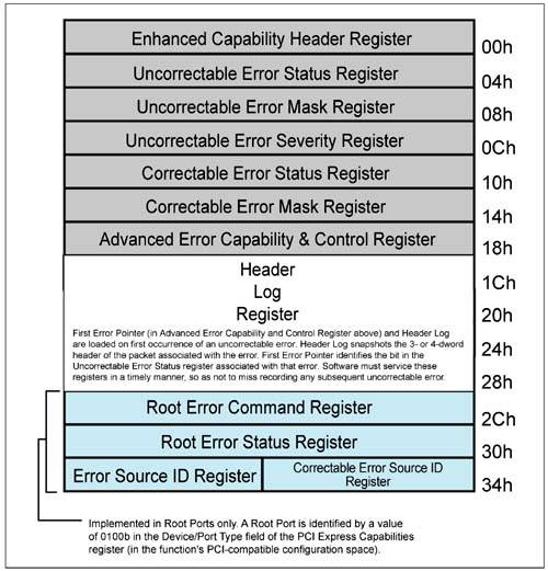
Figure 24-16 on page 931 illustrates the optional Advanced Error Reporting capability register set. Note that the registers in the last three dwords of this register set may only be implemented for a Root Port function (one that has a value of 0100b in the Device/Port Type field of the PCI Express Capabilities register in the function's PCI-compatible configuration space). This capability register set consists of the registers pictured in Figure 24-16 on page 931 and described in Table 24-13 on page 932.
Detailed Description
For a detailed description of the Advanced Error Reporting capability register set, refer to "Advanced Error Reporting Mechanisms" on page 382.
Table 24-13. Advanced Error Reporting Capability Register Set|
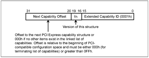
NA | Enhanced Capability Header | Capability ID = 0001h. The Capability Version field in this register is assigned by the SIG and defines the layout of the register set. It must be 1h for all of the extended capabilities currently defined. See Figure 24-17 on page 935.
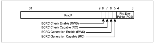
| NA | Capabilities and Control Register | Contains the following bits fields:
First Error Pointer.
Read-only. Identifies the bit position of the first error reported in the Uncorrectable Error Status register (see Figure 24-23 on page 937).
ECRC Generation Capable.
Read-only. 1 indicates that the function is capable of generating ECRC (End-to-End CRC; refer to "ECRC Generation and Checking" on page 361).
ECRC Generation Enable.
Read/write sticky bit. When set to one, enables ECRC generation. Default = 0.
ECRC Check Capable.
Read-only. 1 indicates that the function is capable of checking ECRC.
ECRC Check Enable.
Read/write sticky bit. When set to one, enables ECRC checking. Default = 0.
See Figure 24-18 on page 935.
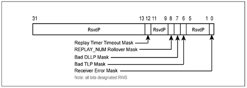
| Correctable Error Registers | Correctable Error Mask Register | Controls the reporting of individual correctable errors by the function to the Root Complex via a PCI Express error message. A masked error (respective bit set to one) is not reported to the Root Complex by the function. This register contains a mask bit for each corresponding error bit in the Correctable Error Status register (see the next row in this table and Figure 24-19 on page 935).
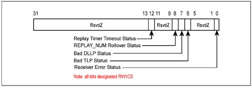
| Correctable Error Status Register | Reports the error status of the function's correctable error sources. Software clears a set bit by writing a 1 to the respective bit. See Figure 24-20 on page 936.
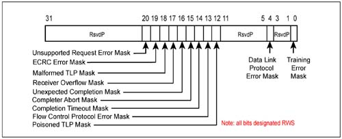
| Uncorrectable Error Registers | Uncorrectable Error Mask Register | Controls the function's reporting of errors to the Root Complex via a PCI Express error message. A masked error (respective bit set to 1b):
is not logged in the Header Log register (see Figure 24-16 on page 931), does not update the First Error Pointer (see the description of the Capabilities and Control Register in this table), and is not reported to the Root Complex.
This register (see Figure 24-21 on page 936)contains a mask bit for each corresponding error bit in the Uncorrectable Error Status register.
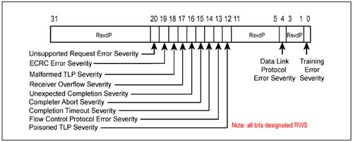
| Uncorrectable Error Severity Register | Each respective bit controls whether an error is reported to the Root Complex via a non-fatal or fatal error message. An error is reported as fatal if the corresponding bit is set to one. See Figure 24-22 on page 937.
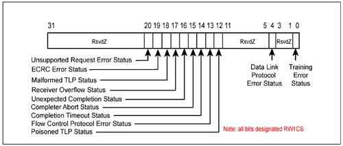
| Uncorrectable Error Status Register | Reports the error status of the function's uncorrectable error sources. See Figure 24-23 on page 937. | Root Error Registers | Root Error Command Register | Controls the Root Complex's ability to generate an interrupt to the processor upon receipt of:
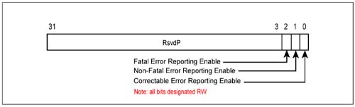
a correctable error message, a non-fatal error message, or a fatal error message
from a child function downstream of the Root Port.
See Figure 24-24 on page 938.
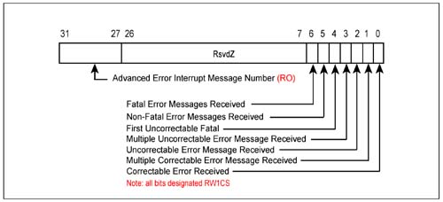
| Root Error Status Register | Tracks the Root Port's receipt of error messages received by the Root Complex from a child function downstream of the Root Port, and of errors detected by the Root Port itself. Non-fatal and fatal error messages are grouped together as uncorrectable. There is a first error bit and a next error bit associated with correctable and uncorrectable errors, respectively. When an error is received by a Root Port, the respective first error bit is set and the Requestor ID is logged in the Error Source Identification register. If software does not clear the first reported error before another error message is received of the same category (correctable or uncorrectable), the corresponding next error status bit will be set, but the Requestor ID of the subsequent error message is discarded. Updated regardless of the settings in the Root Control and the Root Error Command registers. See Figure 24-25 on page 938.
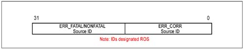
| Uncorrectable Error Source ID Register | Identifies the source (Requestor ID) of the first uncorrectable (non-fatal/fatal) error reported in the Root Error Status register. Updated regardless of the settings in the Root Control and the Root Error Command registers. See Figure 24-26 on page 938.
| Correctable Error Source ID Register | Identifies the source (Requestor ID) of the first correctable error reported in the Root Error Status register. Updated regardless of the settings in the Root Control and the Root Error Command registers. See Figure 24-26 on page 938. |
Virtual Channel Capability
The VC Register Set's Purpose
This register set serves several purposes:
In a port that implements multiple VC buffers, it permits the configuration of the TC-to-VC mapping. See Figure 24-27 on page 939. In an egress port that implements multiple VC buffers, it permits the configuration of the arbitration scheme that defines the order in which each VC accepts packets from the various source ingress ports within the device. This is referred to as the VC's port arbitration scheme.
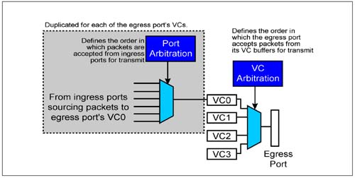
See Figure 24-27 on page 939. In an egress port that implements multiple VC buffers, it permits the configuration of the arbitration scheme that defines the order in which the egress port accepts packets from its VC buffers for transmit onto the link. This is referred to as the port's VC arbitration scheme. In a port that only implements a single VC (VC0), the configuration software may specify that only packets with certain TCs be accepted into the VC0 buffer for transfer. This is referred to as TC filtering.
Who Must Implement This Register Set?
The following functions must implement this optional register set:
A function (i.e., a port) that only implements VC0 but permits the configuration software to specify that only packets with certain TCs may be placed in the VC0 buffer for transfer. A function that implements VCs in addition to VC0.
This applies to Endpoint devices, upstream and downstream Switch ports, Root Ports, and RCRBs.
Multifunction Upstream Port Restriction
The spec contains the following statement:
"The PCI Express Virtual Channel Capability structure can be present in the Extended Configuration Space of all devices or in RCRB with the restriction that it is only present in the Extended Configuration Space of Function 0 for multifunction devices at their Upstream Ports."
The authors take this to mean that if the upstream port of a device is implemented as a multifunction device (see Figure 21-11 on page 761) and that port meets the criteria specified in "Who Must Implement This Register Set?" on page 940, this capability register set is only implemented in the Extended Configuration Space of function 0 of that device.
The Register Set
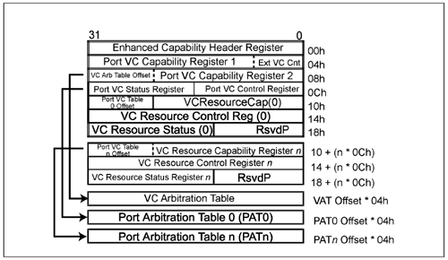
Figure 24-28 on page 941 illustrates the VC Capability register set and Figure 24-29 on page 941 illustrates the detail of its Enhanced Capability Header register.
Detailed Description of VCs
For a detailed description of VCs, refer to Chapter 6, entitled "QoS/TCs/VCs and Arbitration," on page 251.
Port VC Capability Register 1
The register is illustrated in Figure 24-30 on page 942 and each bit field is described in Table 24-14 on page 942.
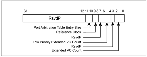
Table 24-14. Port VC Capability Register 1 (Read-Only)|
2:0 | Extended VC Count.
The number of additional VCs supported by the device.
| 6:4 | Low Priority Extended VC Count.
Indicates the number of VCs (starting with VC0) that comprise the Low-Priority VC (LPVC) group.
0. There is no LPVC group and the sequence in which the port's VC buffers transfer is governed by the fixed-priority scheme wherein VC0 has the lowest priority and the highest-numbered VC that is implemented has the highest priority.
Non-zero value (n).
VCs 0-through-n are members of the LPVC group. The value specified cannot be greater than that specified in the Extended VC Count field of this register. - The VCs above n are members of the high-priority group where VCn+1 has the lowest priority and the highest VC has the highest priority. - Control passes to the LPVC group only when the VCs in the upper group have no packets to transfer. The priority scheme used among the VCs that are members of the lower group is governed by the VC Arbitration Capability field in Port VC Capability Register 2 (see "Port VC Capability Register 2" on page 943).
| 9:8 | Reference Clock.
The reference clock for VCs that support time-based WRR Port Arbitration. This field is valid for RCRB and for Switch Ports and is not valid for Root Ports and Endpoint devices (must be hardwired to 0).
| 11:10 | Port Arbitration Table Entry Size.
Indicates the size (in bits) of each entry in the device's Port Arbitration table. This field is valid only for an RCRB and for any Switch Port. It is hardwired to 0 for Endpoint devices and Root Ports.
00b The size of each Port Arbitration table entry is 1 bit. 01b The size of each Port Arbitration table entry is 2 bits. 10b The size of each Port Arbitration table entry is 4 bits. 11b The size of each Port Arbitration table entry is 8 bits.
|
Port VC Capability Register 2
The register is illustrated in Figure 24-31 on page 943 and each bit field is described in Table 24-15 on page 944.

Table 24-15. Port VC Capability Register 2 (Read-Only)|
7:0 | VC Arbitration Capability.
This bit mask indicates the arbitration scheme(s) supported by the device for the LPVC group. It is valid for all devices that report a Low Priority Extended VC Count greater than 0 (see the description in Table 24-14 on page 942). Each bit corresponds to an arbitration scheme defined below. When more than one bit is set, it indicates that the Port can be configured to provide different VC arbitration services.
Bit 0:
Hardwired, fixed arbitration scheme (e.g., Round Robin).
Bit 1:
Weighted Round Robin (WRR) arbitration with 32 phases.
Bit 2:
WRR arbitration with 64 phases.
Bit 3:
WRR arbitration with 128 phases.
Bits 4-7:
Reserved.
The desired arbitration scheme is selected via the VC Arbitration Select field in the Port VC Control Register (see Table 24-16 on page 945). | 31:24 | VC Arbitration Table Offset.
Indicates the location of the VC Arbitration Table with reference to the start of the VC capability register set (specified in increments of dqwords—16 bytes). A value of 0 indicates that the table is not present. |
Port VC Control Register
The register is illustrated in Figure 24-32 on page 944 and each bit field is described in Table 24-16 on page 945.

Table 24-16. Port VC Control Register (Read-Write)|
0 | Load VC Arbitration Table.
In order to activate a port's VC Arbitration Table, the configuration software takes the following steps:
When software initially programs the VC Arbitration Table, or when any change is subsequently made to any entry in the table, the VC Arbitration Table Status bit in the Port VC Status register is automatically set to one by hardware. Software then sets the Load VC Arbitration Table bit to one, causing the port to read the VC Arbitration Table from the capability register set and apply it. When the port hardware has completed reading and applying the updated table, it automatically clears the VC Arbitration Table Status bit in the Port VC Status register. Software can determine if the updated table has been applied by reading the state of the VC Arbitration Table Status bit in the Port VC Status register. - 0 indicates the updated table has been read and applied. - 1 indicates that the update is not yet complete.
This bit is valid for a device when the selected VC Arbitration type (see the next row in this table) uses the VC Arbitration Table. Clearing this bit has no effect. This bit always returns 0 when read. | 3:1 | VC Arbitration Select.
The configuration software selects one of the supported LPVC arbitration schemes by setting it to the BCD value of the bit corresponding to the desired scheme (see the description of bits 7:0 in Table 24-15 on page 944). The configuration software must select the arbitration scheme prior to enabling more than one VC in the LPVC group. |
Port VC Status Register
The register is illustrated in Figure 24-33 on page 946 and each bit field is described in Table 24-17 on page 946.
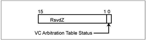
Table 24-17. Port VC Status Register (Read-Only)|
0 | VC Arbitration Table Status.
See the description of the Load VC Arbitration Table bit in Table 24-16 on page 945. |
VC Resource Registers
General
At a minimum, each port implements a single VC, VC0, and it may optionally implement up to eight VCs, VC0-through-VC7. For each VC it supports, the port implements the following three registers:
VC Resource Capability register. VC Resource Control register. VC Resource Status register.
The following three sections provide a description of each of these registers.
Each VC implements:
A mandatory TC/VC bit map that defines the TCs that should be accepted into this VC. An optional Port Arbitration Table that defines the order in which the VC accepts packets from the device ingress ports that source packets to it for transmission.
VC Resource Capability Register
The register is illustrated in Figure 24-34 on page 947 and each bit field is described in Table 24-18 on page 947.
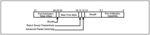
Table 24-18. VC Resource Capability Register|
7:0 | RO | Port Arbitration Capability.
This bit mask indicates the types of Port arbitration (one or more) supported by the VC. It is valid for all Switch Ports and an RCRB, but not for PCI Express Endpoint devices or Root Ports.
Software selects one of these arbitration schemes by writing to the Port Arbitration Select field in the VC Resource Control register (see "VC Resource Control Register" on page 948).
Bit 0.
Hardwired, fixed arbitration scheme (e.g., Round Robin).
Bit 1.
Weighted Round Robin (WRR) arbitration with 32 phases.
Bit 2.
WRR arbitration with 64 phases.
Bit 3.
WRR arbitration with 128 phases.
Bit 4.
Time-based WRR with 128 phases.
Bit 5.
WRR arbitration with 256 phases.
Bits 6-7.
Reserved.
| 14 | RO | Advanced Packet Switching.
1 = This VC only supports transactions optimized for Advanced Packet Switching (AS). This bit is valid for all PCI Express Ports and RCRB. 0 = The VC is capable of supporting all transactions defined by the spec (including AS transport packets).
| 15 | HwInit | Reject Snoop Transactions.
0 = Transactions with or without the No Snoop bit set are allowed on this VC. 1 = Transactions with No Snoop = 0 are rejected as an Unsupported Request. This bit is valid for Root Ports and RCRB, but not for Endpoint devices or Switch ports.
| 22:16 | HwInit | Maximum Time Slots.
Max time slots (minus one) that the VC supports when configured for time-based WRR port arbitration. This field is valid for all Switch ports, Root Ports and an RCRB, but not for Endpoint devices. Only valid when the Port Arbitration Capability field in this register indicates that the VC supports time-based WRR port arbitration. | 31:24 | RO | Port Arbitration Table Offset.
Indicates the location of the Port Arbitration Table associated with this VC with reference to the start of the VC capability register set (specified in increments of dqwords—16 bytes). A value of 0 indicates that the table is not present. This field is valid for all Switch ports and an RCRB, but not for Endpoint devices or Root Ports. |
VC Resource Control Register
The register is illustrated in Figure 24-35 on page 948 and each bit field is described in Table 24-19 on page 949.
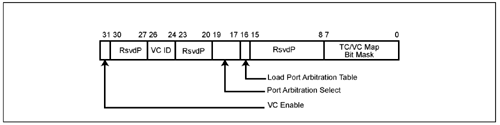
Table 24-19. VC Resource Control Register (Read-Write)|
7:0 | TC/VC Map.
TC-to-VC mapping bit map. Each bit within this field corresponds to a TC that is mapped to this VC. Multiple bits may be set to one. | Bit | 7 | 1 = TC7 is mapped to this VC. | 6 | 1 = TC6 is mapped to this VC. | 5 | 1 = TC5 is mapped to this VC. | 4 | 1 = TC4 is mapped to this VC. | 3 | 1 = TC3 is mapped to this VC. | 2 | 1 = TC2 is mapped to this VC. | 1 | 1 = TC1 is mapped to this VC. | 0 | 1 = TC0 is mapped to this VC. This bit is read-only. 1 for VC0 and 0 for all other enabled VCs. | Before removing one or more TCs from the TC/VC Map of an enabled VC, software must ensure that no new or outstanding transactions with those TC labels are targeted at the given Link.
The default value = FFh for VC0 and = 00h for other VCs. | 16 | Load Port Arbitration Table.
In order to activate a VC's Port Arbitration Table, the configuration software takes the following steps:
When software initially programs the VC's Port Arbitration Table, or when any change is subsequently made to any entry in the table, the Port Arbitration Table Status bit in the VC's VC Resource Status register (see "VC Resource Status Register" on page 950) is automatically set to one. Software then sets the Load Port Arbitration Table bit to one, causing the VC to read the updated Port Arbitration Table from the capability register set and apply it. When the VC hardware has completed reading and applying the updated table, it automatically clears the Port Arbitration Table Status bit in its VC Resource Status register. Software can determine if the updated table has been applied by reading the state of the Port Arbitration Table Status bit in the VC's VC Status register. - 0 indicates the updated table has been read and applied. - 1 indicates that the update is not yet complete.
This bit is valid for a device when the selected Port Arbitration type (the next row in this table) uses the Port Arbitration Table. Clearing this bit has no effect. This bit always returns 0 when read. This bit is valid for all Switch Ports and an RCRB, but not for Endpoint devices or Root Ports. This bit always returns 0 when read and the default value of this bit is 0. | 19:17 | Port Arbitration Select.
The configuration software selects one of the supported port arbitration schemes by setting it to the BCD value of the bit corresponding to the desired scheme (see the description of bits 7:0 in Table 24-18 on page 947). The configuration software must select the arbitration scheme prior to enabling more than one VC in the LPVC group. | 26:24 | VC ID.
This field assigns a VC ID (between 0 and 7) to the VC (for VC0, it is hardwired to zero). It cannot be modified if the VC has already been enabled. | 31 | VC Enable.
1 = VC enabled. 0 = VC disabled.
The state of this bit is qualified by the state of the VC Negotiation Pending bit (in the VC's VC Resource Status register; see "VC Resource Status Register" on page 950).
0 = negotiation has been completed (Flow Control initialization is completed for the PCI Express Port) and the VC Enable bit indicates the state of the VC. 1 = the negotiation process has not yet completed and the state of the VC Enable bit therefore remains indeterminate.
This bit is hardwired to 1 for VC0. It is read/write for the other VCs and its default is 0.
To enable a VC, its VC Enable bit must be set to one in the ports at both ends of the link.
To disable a VC, its VC Enable bit must be cleared to zero in the ports at both ends of the link.
Before disabling a VC, software must ensure that no traffic is using the VC.
Prior to re-enabling a VC, software must first fully disable the VC in both components on the Link. |
VC Resource Status Register
The register is illustrated in Figure 24-36 on page 951 and each bit field is described in Table 24-20 on page 951.
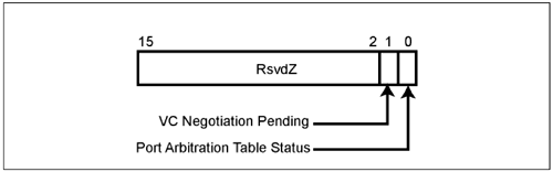
Table 24-20. VC Resource Status Register (Read-Only)|
0 | Port Arbitration Table Status.
See the description of the Load Port Arbitration Table bit in Table 24-19 on page 949. The default value of this bit is 0. | 1 | VC Negotiation Pending.
Indicates whether the VC negotiation process (initialization or disabling) is in the pending state. When this bit is set by hardware, it indicates that the VC is still in the process of negotiation. It is cleared by hardware after the VC negotiation completes. For VCs other than VC0, software uses this bit to enable or disable the VC. For VC0, this bit indicates the status of the Flow Control initialization process. Before using a VC, software must check whether the VC Negotiation Pending bit is cleared in the components at both ends of the Link. |
VC Arbitration Table
A port implements a VC Arbitration Table if both of the following are true:
The table consists of a set of read/write registers and is only used if the configuration software selects (via the VC Arbitration Select field in Table 24-15 on page 944) one of the implemented WRR VC arbitration schemes (see VC Arbitration Capability in Table 24-15 on page 944).
The configuration software configures the table with the arbitration scheme that the egress port logic uses to service the VC transmit buffers associated with the port. See the description of the Load VC Arbitration Table bit in Table 24-16 on page 945 for a description of how the table is uploaded into the port's logic. For a detailed description of the VC Arbitration Table, refer to "Loading the Virtual Channel Arbitration Table" on page 270.
Port Arbitration Tables
A VC implements a Port Arbitration Table if both of the following are true:
The table consists of a set of read/write registers and is only used if the configuration software selects (via the Port Arbitration Select field in Table 24-19 on page 949) one of the implemented WRR Port arbitration schemes (see Port Arbitration Capability in Table 24-18 on page 947).
The configuration software configures the table with the arbitration scheme that defines in what order the VC accepts packets being sourced from the ingress ports that have packets to be passed to this VC buffer on the egress port. See the description of the Load VC Arbitration Table bit in Table 24-16 on page 945 for a description of how the table is uploaded into the port's logic.
This register array is valid for all Switch Ports and RCRBs, but not for Endpoint devices or Root Ports. For a detailed description of the Port Arbitration Tables, refer to "The Port Arbitration Mechanisms" on page 277.
Device Serial Number Capability
This optional register set can be implemented on any PCI Express device in accordance with the following rules:
It consists of the Enhanced Capability Header pictured in Figure 24-37 on page 953 and the 64-bit Serial Number register pictured in Figure 24-38 on page 953.
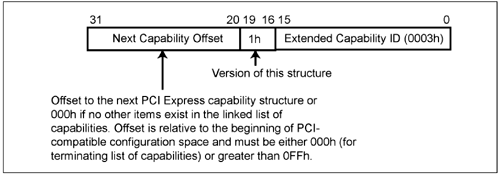
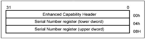
The device serial number is a unique, read-only 64-bit value assigned to the device when it is manufactured. A multifunction device with this feature only implements it on function 0 and other functions within the device must return the same serial number value as that reported by function 0. Any component (e.g., a Switch) that contains multiple devices must return the same serial number for each device within the component.
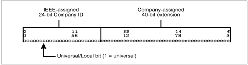
The serial number is also known as the EUI-64. Refer to Figure 24-39 on page 954. A portion of the Extended Unique Identifier (EUI)-64 is assigned by a registration authority operating under the auspices of the IEEE organization. The EUI-64 consists of:
24-bit company ID value assigned by IEEE. Bit 6, the Universal/Local scope bit, is always set to one (Universal scope ID, not assigned to anything else in the universe) in the value assigned by the IEEE. 40-bit extension ID assigned by the company that "owns" the assigned company ID. The interpretation of the company-assigned extension is outside the scope of the spec. As an example, it may represent the device ID and manufacturer-assigned serial number.
Power Budgeting Capability
General
Refer to Chapter 15, entitled "Power Budgeting," on page 557 for a detailed description of the Power Budgeting capability.
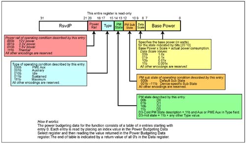
This optional capability permits the platform to properly allocate power to a device that is hot-plugged into the system during runtime. Using this register set, the device reports the following to the platform:
The power it consumes on a variety of power rails. The power it consumes in different power management states. The power it consumes under different operating conditions.
The platform (i.e., the system and the OS) uses this information to ensure that the system can provide the proper power and cooling levels to the device.
Implementation of this capability register set (see Figure 24-40 on page 955) is optional for devices that are implemented either in a form factor which does not require hot-plug support, or that are integrated on the system board. Although the spec states that "PCI Express form factor specifications may require support for power budgeting," it does not indicate any specific cases where this is required.
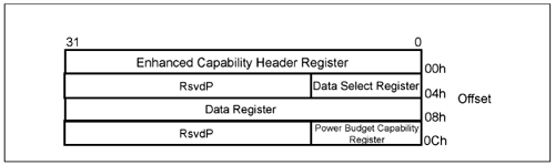
Figure 24-40 on page 955 illustrates the register set and Figure 24-41 on page 955 illustrates its Enhanced Capability Header register.
How It Works
The power budgeting data for the function consists of a table of n entries starting with entry 0. Each entry is read by placing an index value in the Power Budgeting Data Select register (Figure 24-40 on page 955) and then reading the value returned in the Power Budgeting Data register (Figure 24-42 on page 956).The end of table is indicated by a return value of all 0's in the Data register.
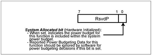
In the Power Budgeting Capability register (see Figure 24-43 on page 956), the System Allocated bit is automatically set to one if the device is integrated onto the system board and its power requirements are therefore already taken into account in the system's power supply budget. In that case, the device's power requirements should be ignored by software in making power budgeting decisions.
 | 
